 +86 755 2794 4155
  sales@knownpcb.com
-
Shenzhen KNOWNPCB Technology Co., Ltd.
 +86 755 2794 4155
  sales@knownpcb.com
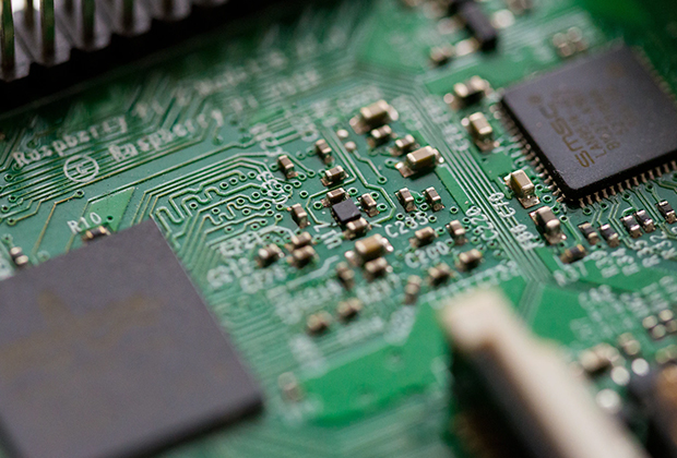
Have you noticed that now more and more of our lighting is using led lighting.What is LED? Compared to the traditional light bulbs, LEDs have lower power consumption, longer lifetime and higher energy efficiency. In the PCB industry,when we say LED PCB, it refers to the pcb used for LED lighting, if you are looking for a suitable LED PCB for your lighting system, this article may bring you something. WHAT ARE LEDS COMPOSED OF?LED is an initial light-emitting diode that produces light when an electric current passes through. LEDs typically have negative and positive electrodes, which generate light in the visible light region.The LEDS are glued to the PCB by soldering process and have electrical connections for lighting.Since light-emitting diodes dissipate a lot of heat when they are in use, when you are designing LED, the metal core is usually the best choice for LED PCB, it is because that it dissipates heat more faster. Among them, the metal material aluminum is the most widely used
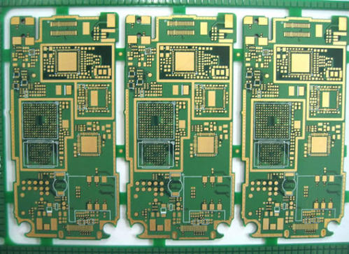
If analog circuits (RF) and digital circuits (microcontrollers) work separately, they may work well on their own, but once they are placed on the same circuit board and powered by the same power source, the entire system is likely to become unstable. This is mainly due to the frequent oscillation of digital signals between ground and positive power supply (3 V in size), and the period is particularly short, often at the ns level. Due to their large amplitude and small switching time, these digital signals contain a large number of high-frequency components that are independent of the switching frequency. In the simulation part, the signal transmitted from the antenna tuning loop to the wireless device receiving part is generally less than 1 μ V. Therefore, the difference between digital signals and RF signals will reach 10-6 (120 dB). Obviously, if digital signals cannot be well separated from radio frequency signals, weak radio frequency signals may be damaged, which can deteriora
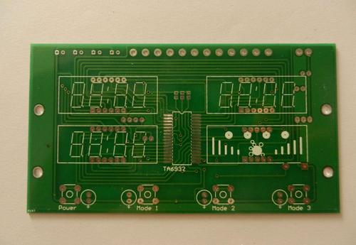
1. When marking and making PCB sample slices, you should first know whether your slice is a transverse or longitudinal section of the hole, and where the problem lies. It must be marked with a colored oil pen or tape. Use an arrow to indicate the problem point 2. For circuit board sampling and gluing, if there are bubbles in the holes, the slice has lost its meaning. Therefore, gluing is the foundation of PCB sampling and slicing. The transparent glue used by everyone may be different, but it is only powder glue or blue and white glue There is always a component that is' rare ' Before gluing, please ensure that the sample is clean, otherwise there will definitely be bubbles generated. The method I use is to wipe and clean with a cotton swab dipped in acetone, or use ultrasonic cleaning Then wet it with a "dilute" solvent Or first dilute the glue and carefully fill the small hole with a toothpick Especially blind holes, carefully fill them with toothpicks, and then fill them with t
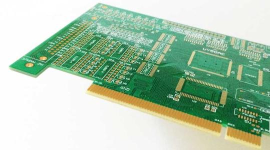
Regardless of the performance of the soldering flux, it will be more or less corrosive. The residue after soldering the circuit board can cause different problems such as corrosion, leakage, and ion migration. Therefore, removing the residue of soldering flux will certainly be regarded as an important processing task by the industry. And what is the actual effect of the processing? Appropriate methods are also needed for verification and tracking in this regard. The cleaning effect of PCB circuit board after soldering should be based on the amount of residual ion residue at the solder joints. The specification adopted by MIL is MIL-P-2880955110, which should have a resistivity of 6MQ-cm or above during testing. Calculate the resistivity of the measured metal per unit area and after quantitative cleaning. In terms of cleanliness, the resistivity should be maintained above 2MQ-cm. Representative cleanliness testing methods include Ion Ogurafu and Omega Meter, which are recognized as

Standard for PCB sampling and substrate testing methods: 1. IEC61189-1 (1997-03): Test methods for electronic materials, interconnecting structures and components - Part Y: General test methods and methodology. 2. IEC61189 (1997-04) Test Methods for Electronic Materials, Interconnected Structures and Components - Part 2: Test Methods for Interconnected Structure Materials, Revised Y in January 2000 3. IEC61189-3 (1997-04) Test Methods for Electronic Materials, Interconnection Structures and Components - Part 3: Test Methods for Interconnection Structures (Printed Boards), revised Y in July 1999. 4. IEC60326-2 (1994-04) Printed boards - Part 2; The experimental method was revised Y times in June 1992. PCB sampling related material standards 1. IEC61249-5-1 (1995-11) Interconnection structural materials - Part 5: Specification for uncoated conductive foils and films - Part Y: Copper foil (used for manufacturing copper-clad substrates) 2. IEC61249-5-4 (1996-06) Printed boards a
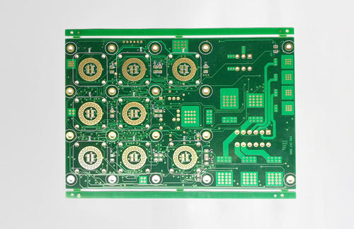
Printed circuit board (PCB) is almost present in every electronic device. If there are electronic components in a certain device, they are also embedded on PCBs of different sizes. In addition to fixing various small parts, the main function of PCB is to provide electrical connections between the various components on top. As electronic devices become increasingly complex and require more and more parts, the circuits and components on the PCB are also becoming denser. A standard PCB looks like this. Bare board (without components on top) is also commonly referred to as "Printed Wiring Board (PWB)". The substrate of the board itself is made of insulated and non bendable materials. The small circuit material visible on the surface is copper foil. Originally, the copper foil covered the entire board, but during the manufacturing process, some parts were etched away, leaving behind a network of small circuits. These circuits are called conductor patterns or wiring, and are used to pro
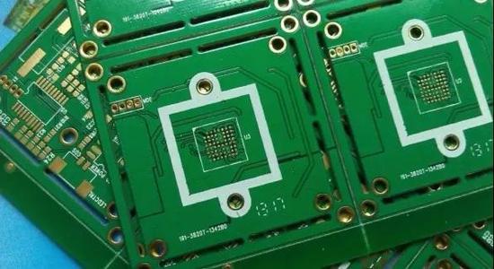
Copper clad laminate (CCL), also known as copper-clad laminate, is a product made of wood pulp paper or fiberglass cloth as reinforcing materials, impregnated with resin, and covered with copper foil on one or both sides, and then hot pressed. When used in the production of multi-layer boards, it is also called a core board (CORE). At present, the copper-clad laminates available in the market can be mainly divided into the following categories based on substrate: paper substrate, fiberglass cloth substrate, synthetic fiber cloth substrate, non-woven fabric substrate, and composite substrate. The circuit board prototype substrate is an insulating layer board composed of polymer synthetic resin and reinforcing materials; A layer of pure copper foil with high conductivity and good weldability is covered on the surface of the substrate, commonly with a thickness of 35-50/ma; Copper clad laminates with copper foil covering one side of the substrate are called single-sided copper clad
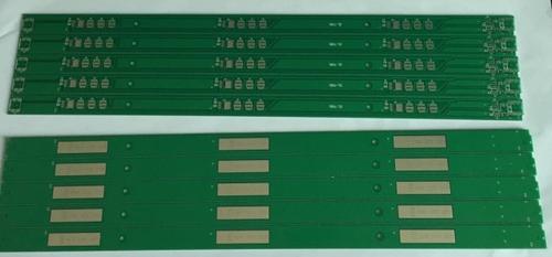
Printed Circuit Board Assembly (PCA) refers to the process of soldering electronic components onto a printed circuit board (PCB). This service is usually provided by professional electronic manufacturing service providers (EMS), covering the entire process from component procurement, inspection, mounting to final testing and quality control. PCA services are widely used in the field of electronic product manufacturing, including multiple industries such as consumer electronics, communication equipment, medical instruments, automotive electronics, and aerospace. In circuit board assembly services, common process flows include surface mount technology (SMT), through-hole insertion technology (THT), and hybrid assembly technology. SMT is suitable for the installation of high-density and miniaturized components, while THT is commonly used for the installation of large or heavy-duty components. Hybrid assembly technology is the combination of SMT and THT to meet the installation needs
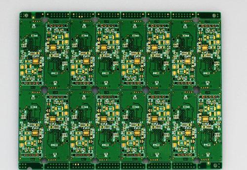
Printed Circuit Board Assembly (PCBA) refers to a printed circuit board that has been assembled and soldered, containing various electronic components. It is the process of making a PCB board from a designed circuit diagram through plate making, etching, drilling, and other processes, and then soldering various electronic components (such as resistors, capacitors, transistors, integrated circuits, etc.) onto the PCB board according to the requirements of the circuit design, forming electronic modules or systems with specific functions. PCBA is the core part of modern electronic product manufacturing, widely used in various fields such as consumer electronics, communication equipment, industrial control, medical instruments, automotive electronics, etc. It not only achieves the integration and miniaturization of electronic components, but also improves the stability and reliability of circuits, simplifying the assembly and maintenance process of electronic products. In the product

Prototype circuit board components are important tools for electronic engineers and enthusiasts when developing new products or conducting electronic experiments. These components typically include various electronic components such as resistors, capacitors, inductors, transistors, integrated circuits, etc. During the design phase, engineers need to select and test various components to ensure the performance and reliability of the final product. The quality of prototype circuit board components directly affects the stability and efficiency of the entire system, so selecting high-quality components is crucial. In practical operation, engineers will use breadboards or test boards to build prototype circuits, which can not only quickly verify the feasibility of circuit design, but also facilitate modification and optimization. Through continuous experimentation and adjustment, engineers can find the best combination of components to achieve the expected functionality and performance
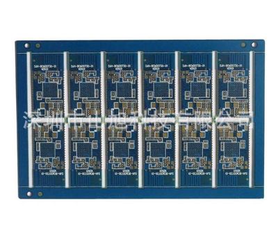
Prototype PCB assembly is a crucial step in the electronic manufacturing process, which involves combining the designed circuit board with various electronic components to form a functional electronic device. This process not only requires professional technical knowledge, but also high precision and meticulous operation. In the prototype stage, manual assembly is usually used to ensure that each component can be installed and welded correctly. When assembling the prototype PCB, it is necessary to first prepare all the components and tools. Components include resistors, capacitors, chips, etc., while tools include soldering, soldering iron, tweezers, magnifying glasses, etc. Next, according to the circuit design drawings, install each component onto the PCB one by one. This step requires the operator to have good vision and hand eye coordination skills, as components are very small, especially SMD (Surface Mount Devices) commonly used in modern electronic products. After installa
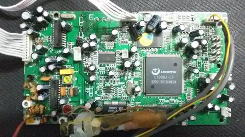
Prototype assembly refers to assembling electronic and mechanical components from various parts into a complete prototype product. This not only includes the installation and welding of electronic components, but also the assembly of mechanical parts such as casings, connecting wires, buttons, etc. Prototype assembly is a complex process that requires multiple skills and experience. In the prototype assembly process, the first step is to ensure the quality and compatibility of all components. Next, according to the design drawings, gradually assemble the various components together. During this process, some adjustments and modifications may need to be made to ensure that the final product works properly and has a good user experience. After assembly, a series of tests are required, including functional testing, performance testing, and reliability testing, to ensure that the product's various indicators meet expectations.

PCB reverse engineering is a technical process through which the design and functionality of existing printed circuit boards can be obtained and understood. This process typically involves disassembling and analyzing the original circuit board in order to replicate its functionality or make improvements. In many cases, reverse engineering is used for product replication, repair, upgrade, or intellectual property analysis. The steps include: first, taking photos and recording the circuit board, including the position and connection method of each component. Then, use chemical solvents to remove solder and components from the circuit board, in order to observe the copper foil routing more clearly. Next, recreate the schematic and layout of the circuit board through scanning or manual drawing. Finally, using this information, the same circuit board can be redesigned or manufactured.
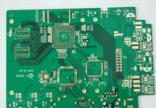
LCD splicing screen users usually don't know how to deal with problems encountered during use, especially when it comes to splicing screens that are out of warranty. This time, let's talk about the aging problem of LCD splicing screens, hoping to help everyone. LCD splicing screens can easily overheat certain pixels due to prolonged operation. Once exceeded, it can lead to fatigue damage, which is commonly known as "bad pixels". Due to the fact that the pixels of the LCD splicing screen are composed of liquid crystals, when it operates continuously at full load for more than 96 hours, it will accelerate its aging, and in severe cases, it may even burn out. No matter what problems occur with the LCD splicing screen, it is forbidden to assemble the LCD splicing screen by yourself. Once the LCD splicing screen does not work properly, you can seek help from the manufacturer to solve it. Due to the fact that the transformer in the LCD background lighting component may still carry a hi
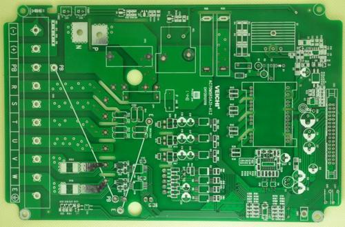
The Main PCB is the core component in electronic devices, carrying the main electronic components and circuits. It is usually located at the center of the device and communicates with other sub circuit boards or modules through connectors. The design and layout of the main PCB directly affect the performance and reliability of the entire system. When designing the main PCB, engineers need to consider multiple factors comprehensively, including circuit layout, signal integrity, power distribution, thermal management, and mechanical structure. Reasonable layout can reduce signal interference and energy loss, improve system stability and efficiency. The design of the power distribution network is also crucial to ensure stable power supply to all parts. The main PCB usually adopts a multi-layer structure to facilitate complex wiring and functional zoning. Common layers include 4, 6, 8, etc. Each layer is connected through through holes and vias to achieve electrical connections and s
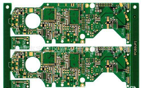
Circular printed circuit board is a special shaped circuit board mainly used in some specific application scenarios, such as circular displays, rotary encoders, circular antennas, etc. Compared with traditional rectangular circuit boards, circular circuit boards have some unique challenges and advantages in design and manufacturing. When designing a circular printed circuit board, engineers need to consider the impact of its special geometric shape on circuit layout and signal transmission. Due to the limited edge length of circular boards, the wiring space is relatively small, which requires more compact and efficient circuit design. In addition, special attention should be paid to the continuity and stability of signals in rotating applications of circular circuit boards to avoid signal interruption or interference caused by rotation. The process of manufacturing a circular printed circuit board is similar to that of a regular circuit board, but requires additional steps to han

Ordinary printed circuit boards (PCBs) are an indispensable part of modern electronic devices. It forms complex circuit patterns by etching copper wires onto an insulating substrate, thereby connecting and supporting various electronic components. This type of circuit board typically consists of several layers, including a top layer, a bottom layer, and an inner layer. The more layers there are, the more complex the functions of the circuit board become, and the corresponding cost increases. When designing a regular printed circuit board, engineers need to consider multiple factors such as circuit layout, signal integrity, power management, etc. The circuit layout determines the arrangement of components and the direction of wires, directly affecting the performance and reliability of the circuit. Signal integrity refers to the degree to which a signal maintains its original shape during transmission, which is particularly important for high-speed circuits. Power management involv
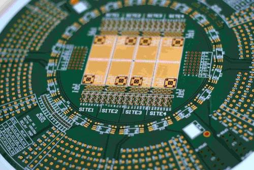
With the increasing global awareness of environmental protection, ROHS (Restriction of Hazardous Substances) standards have become an important norm in the electronics industry. Our company actively responds to the call for environmental protection and has launched printed circuit boards (ROHS PCBs) that comply with ROHS standards. These circuit boards not only have excellent electrical performance, but also strictly limit the use of harmful substances to ensure minimal impact on the environment. Our ROHS printed circuit board uses lead-free solder, halogen-free materials, and low pollution chemical treatment processes. In the production process, we strictly comply with environmental regulations and reduce environmental pollution through advanced waste treatment systems and resource recycling technologies. In addition, we have also obtained multiple international environmental certifications to ensure that the environmental performance of our products reaches the international adv
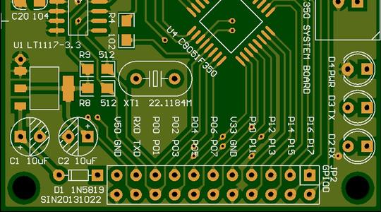
Printed Circuit Board (PCB) is an essential core component in modern electronic devices. It achieves efficient layout and functional integration of complex circuits by connecting electronic components together. In the design and manufacturing process, we strictly follow industry standards to ensure that every PCB has excellent performance and reliability. Our PCB adopts advanced production processes, including high-precision laser drilling, precise etching technology, and high-quality surface treatment processes. The application of these technologies not only improves the conductivity of the circuit board, but also enhances its anti-interference ability and durability. We are committed to providing customers with the best product solutions for both single-layer and multi-layer boards. In addition, we have an experienced team of engineers who are proficient in various circuit design software and can customize designs according to customer needs. We provide technical support throug
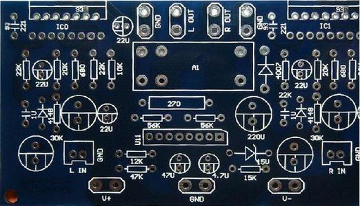
Printed Circuit Board (PCB) is an essential core component in modern electronic products. It connects various electronic components such as resistors, capacitors, transistors, etc. by printing conductive patterns on an insulating substrate to achieve circuit functionality and signal transmission. The application range of PCB is extremely wide, from household appliances to aerospace equipment, almost all electronic devices cannot do without its support. The main advantage of PCB lies in its high-density integration and automated production. Through multi-layer stacking and precision machining techniques, complex circuit designs can be achieved in limited space, greatly improving the performance and reliability of electronic devices. In addition, the standardized production and testing process of PCBs ensures high quality and consistency of products, reducing manufacturing costs and cycles. During the design and manufacturing process, engineers use professional EDA software for cir
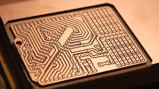
Printed Circuit Board (PCB) is the heart and nerve center of modern electronic products. It achieves electrical connection and signal transmission between electronic components by printing conductive circuits on insulating substrates. The widespread application and importance of printed circuit boards (PCBs) make them the foundation and core of modern electronics industry. The main functions of a printed circuit board (PCB) include electrical connections, signal transmission, and component support. By installing various electronic components such as resistors, capacitors, transistors, and integrated circuits on circuit boards, electronic products can achieve complex functions and efficient operation. The manufacturing process of printed circuit boards (PCBs) is very complex, including multiple steps such as circuit design, substrate selection, copper foil etching, drilling, and surface treatment. Each step requires strict quality control and precise process technology. With the c
Inquiry Now

