Summary
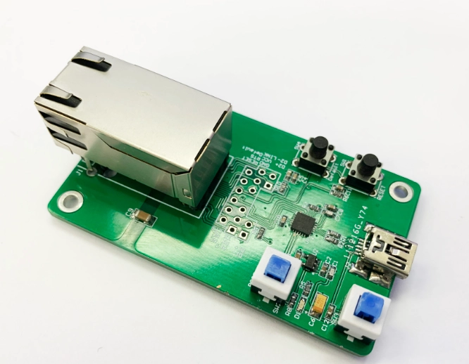
Heavy or large-footprint components, such as large transformers, large inductors, electrolytic capacitors, heatsinks, shield cans, or board-edge connectors, can cause the risk which is not only component weight. It is alsocombined with narrow bridges, V-cuts, irregular-shaped boards, or weak panel support. In this case, the PCB board may pass Gerber checks but still face warpage, bridge breakage, solder joint cracks, or depaneling damage during SMT, transportation, or mass production.
If a PCB design includes plated slots, complex outlines, or narrow bridge areas, it is better to involve the factory early in the DFM/CAM manufacturability review.
A better review point is after the structural plan is confirmed and before the formal layout is fully finalized. These structural details may look small at first, but they can influence process capability, process selection, panel strength, SMT stability, and mass production yield.
DFM/CAM Manufacturability Review Timing
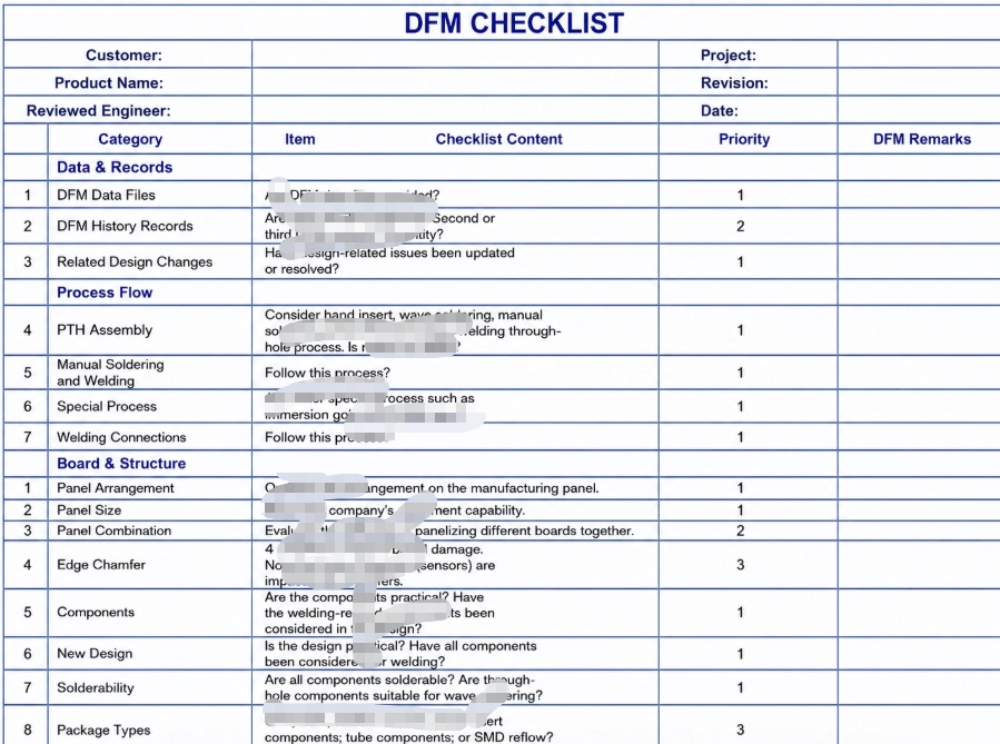
For PCB projects with plated slots, complex outlines, or narrow bridge areas, the DFM/CAM manufacturability review should usually be placed after the structural plan is confirmed and before the formal PCB layout is finalized.
When Should the Factory Review a PCB Design with Plated Slots, Complex Outlines, or Narrow Bridges?
The PCB factory should run an early DFM review to prevent design rework and unnecessary PCB design version changes. The preferred timing is after the structural scheme is confirmed and before the PCB layout is finalized.
This matters because these PCB design decisions directly affect the manufacturer’s process capability and process selection:
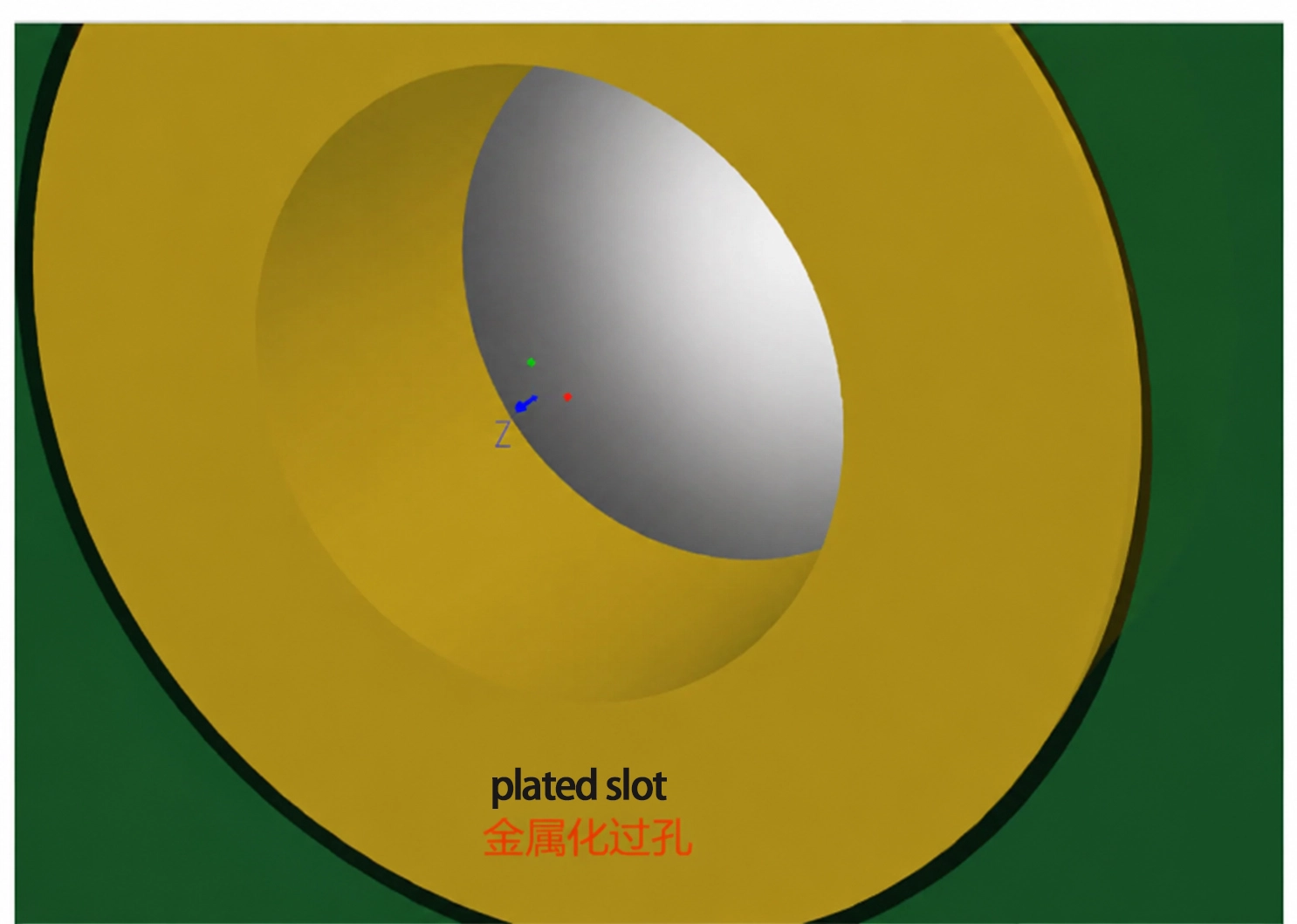
- Plated slots: minimum plated-through slot width, required slot dimensions, copper lining, slot milling method, and plating capability.
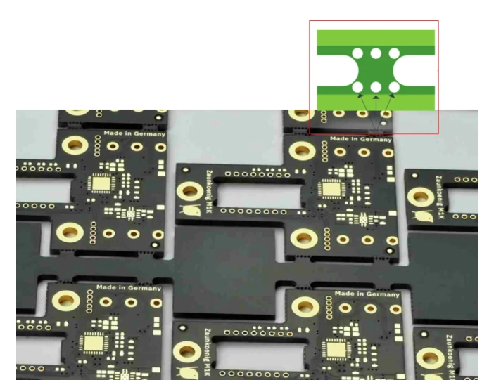
- Complex and irregular outlines: CNC routing, machining tolerance, panelization method, V-cut, mouse-bite tabs, and bridge connection solutions.
- Narrow bridge areas: panel strength, deformation risk during transportation and SMT, depaneling method, and minimum remaining bridge width.
Confirmation of Plated Slot Processing Capability
Before layout release, the review should verify the minimum machinable slot width, slot-wall plating capability, finished copper thickness, and compensation method.
What to Check If the PCB Project Includes Plated Slots, Irregular Board Shapes, and Narrow Bridge Structures?
- Minimum machinable slot width, slot-wall plating capability, hole/slot copper thickness, and compensation method for plated slots.
- Routing paths, machining tolerances, edge burr control, and panelization feasibility for irregular board shapes.
- Minimum remaining bridge width, number of bridges, SMT reflow stability, and transportation strength.
- Whether V-cut, mouse-bite tabs, or routed depaneling methods restrict the irregular structure.
- Risks of bridge breakage, warpage, edge chipping, insufficient hole copper, panel damage, or reduced yield.
Factories should provide feedback on process capability limits, suggested modifications, and mass production risks.
Confirm the Method for Irregular Boards and Panelization
Complex irregular structures require a full review of CNC routing paths, tolerances, tab routing, and depaneling solutions.
The Risk of Narrow Bridge in Plated-Hole Design Requirements
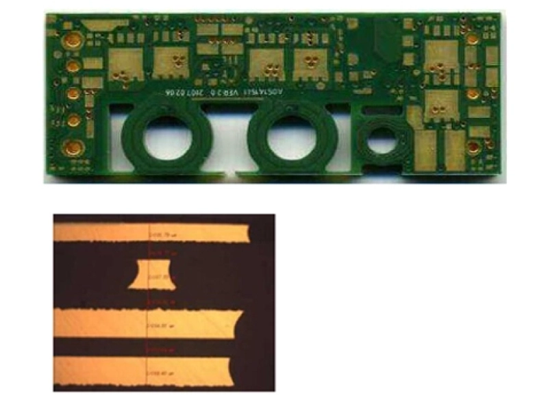
In plated-hole design requirements, one common issue is that the small bridges connecting a single board to edge rails or adjacent boards are very narrow. At present, the lower limit for a narrow bridge is 0.15 mm, or 6 mil, which is considered the minimum safe width for stable PCB mass production.
However, the risk becomes higher when the single board carries heavy components, force-bearing components, high-thermal-mass components, or parts with a shifted center of gravity.
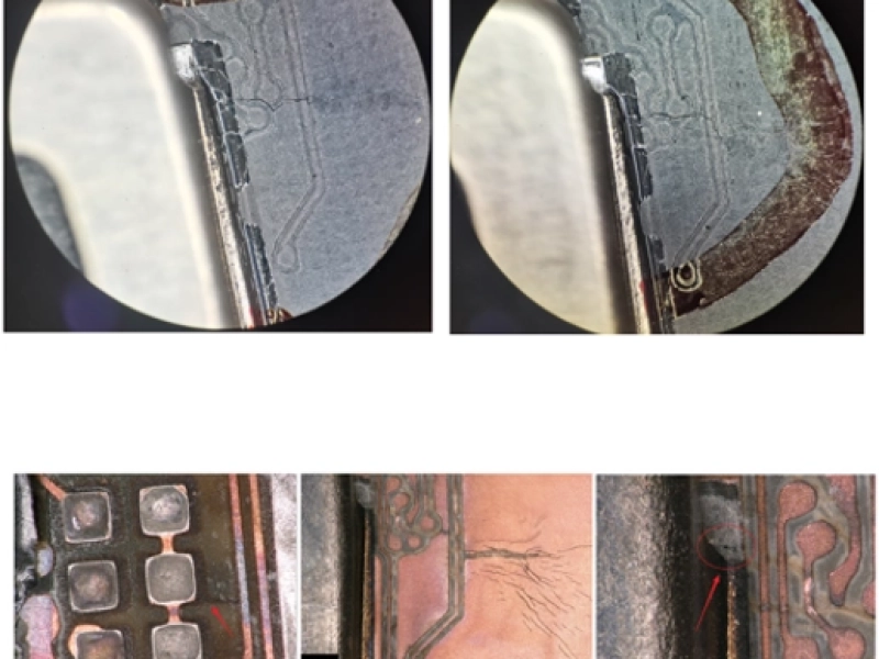
Too-weak tabs can lead to bridge breakage, warpage, local stress cracking, or solder joint cracks. These production risks may occur during SMT assembly, reflow soldering, transportation, or depaneling.
The following combinations should be marked as high risk and require CAM + SMT engineering review.
For example, some PCB design standards prohibit bridges below 0.2 mm under BGAs. They may require mouse-bite tabs, micro-connection structures, and at least four bridge points.
Core Conclusion
- “Force concentration” is a physical result of the geometric structure, not a process defect.
- Kt≈5 at a 0.15 mm bridge area is the critical point where stress concentration shifts from acceptable to high risk.
- The edge of the plated hole wall is the main stress concentration area. Thermal stress from large components, such as BGAs or inductors, can trigger fatigue crack growth in this area.
When heavy components, board-edge interfaces, irregular outlines, or V-cuts are combined with narrow bridges, panel strength and depaneling reliability risks increase significantly.
| Combination | Risk Level | Reason |
|---|---|---|
| Narrow bridge + RJ45/USB/terminal block near the board edge | High | Insertion and pull-out forces concentrate edge stress. |
| Narrow bridge + large inductor/transformer | High | Heavy components increase warpage risk during reflow and transportation. |
| Narrow bridge + large electrolytic capacitor | Medium-high | A higher center of gravity increases vibration and depaneling risk. |
| Narrow bridge + heatsink/shield | High | Weight, thermal mass, and expansion stress accumulate together. |
| Narrow bridge + screw post/riveted parts | High | Mechanical locking stress may cause local cracks. |
| Narrow bridge + irregular board shape | High | Panel support may be insufficient. |
| Narrow bridge + V-cut | High | V-cut weakens the remaining bridge strength. |
| Narrow bridge + heavy components close to the bridge area | High | The bridge area carries the highest local load. |
| Narrow bridge area + large thin board | High | Warpage and bridge breakage risks increase. |
KnownPCB’s Perspective
From the perspective of manufacturing feasibility and mass production stability, plated slots, complex outlines, and narrow bridges should not be treated as manufacturing afterthoughts. KnownPCB recommends introducing DFM/CAM review during the PCB layout phase and before formal layout finalization.
This helps identify PCB fabrication machining limits, panel strength risks, SMT reflow issues, and depaneling risks earlier. It also reduces late-stage rework and yield fluctuation during PCB mass production. For PCB projects with plated slots, irregular outlines, narrow bridges, and heavy component combinations, joint review by the PCB factory and SMT engineers is a more reliable path to mass production.