Leading technology
1.Minimum line w/s 3mil/3mil, minimum aperture 0.075mm.
2.FR4+ high frequency mixed pressure, high frequency multistage step plate, metal base, etc
3.Mechanical blind burring, HDI, rigid torsion combination and other processing technology.
Advanced research and development strength
1.10 years' experience in R&D and manufacturing of medical printed circuit boards, including medical diagnosis, patient intelligent drug injection, patient intelligent monitoring system, X-ray machine, B-ultrasound machine, blood glucose meter, etc.
2.Assist customers to develop new products such as endoscope, scalpel and lifting beds.
3.Production of multiple high level HDI and rigid flexible joint and other processing technologies.
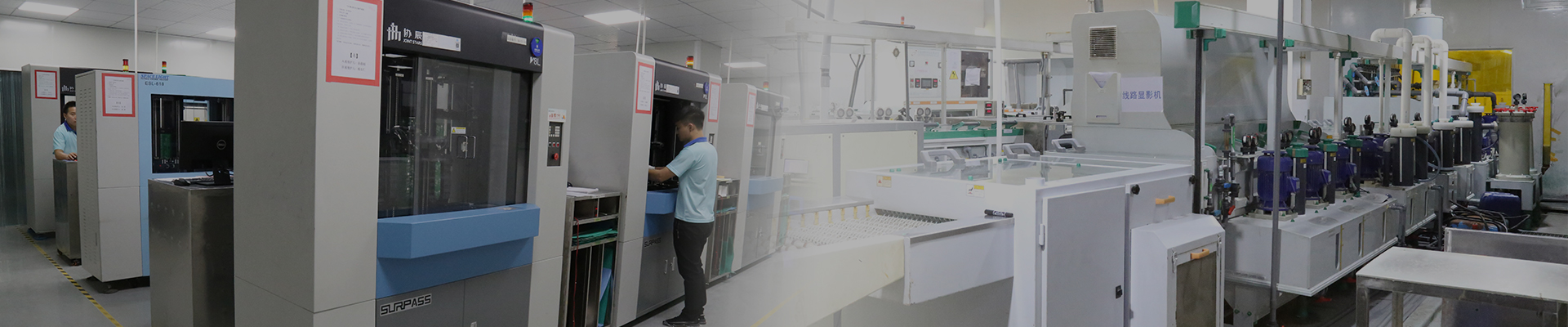
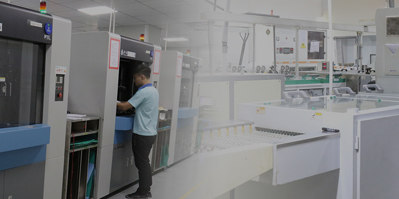
Advanced production equipment&Complete quality control system
1.100% of products have been tested by imported AOI to reduce electrical leakage and ensure that the inductance of power products meets customer design requirements.
2.More than 20 kinds of reliability testing equipment, such as reflow welding, thermal shock, pore copper tester, impedance tester, gold-nickel thickness tester, etc.
3.ISO9001, ISO14001, AITF16949, UL, CQC quality system certification, etc
4.Strictly implement quality PDCA process and continuously improve product performance.
5.Strictly follow IPQP,SPC,FMEA,MSA and PPAP system operation.
 +86 755 2794 4155
  sales@knownpcb.com
 EN
EN CN
CN
 Home >


