 +86 755 2794 4155
  sales@knownpcb.com
-
Shenzhen KNOWNPCB Technology Co., Ltd.
 +86 755 2794 4155
  sales@knownpcb.com
Have you noticed that now more and more of our lighting is using led lighting.What is LED? Compared to the traditional light bulbs, LEDs have lower power consumption, longer lifetime and higher energy efficiency. In the PCB industry,when we say LED PCB, it refers to the pcb used for LED lighting, if you are looking for a suitable LED PCB for your lighting system, this article may bring you something. WHAT ARE LEDS COMPOSED OF?LED is an initial light-emitting diode that produces light when an electric current passes through. LEDs typically have negative and positive electrodes, which generate light in the visible light region.The LEDS are glued to the PCB by soldering process and have electrical connections for lighting.Since light-emitting diodes dissipate a lot of heat when they are in use, when you are designing LED, the metal core is usually the best choice for LED PCB, it is because that it dissipates heat more faster. Among them, the metal material aluminum is the most widely used
Many people have misunderstandings about the concept of PCB copy plate. In fact, with the continuous development and deepening of the copy of the board industry, today’s PCB copy concept has been extended widely, and it is no longer limited to the copy and cloning of simple circuit boards and cloning. It will also involve the second development of the product and the development of new products. For example, through the analysis of existing product technical documents, design ideas, structural characteristics, process technology, etc., you can provide feasibility analysis and competitive reference for the research and development and design of new products, and assist R & D design units to follow up the latest. The technological development trend, timely adjust the improvement of product design plans, and develop the most competitive new products in the market. At the same time, the process of PCB copy plate through the extraction and partial modification of the technical data file
In the 1980s, Western capitalist countries vigorously developed technology, and various high -end technology electronics products came into being. Such electronic products are widely used. Product developers have its full set of technical solutions to monopolize the technical solutions of such products. Some companies developing products have even maliciously raised their products to obtain greater profits. In this monopoly environment, some companies have tried to break this monopoly, gain profits from it, try to imitate such products, and do reverse research and analysis of these high -tech products, which is what we call PCB copy board. The PCB copy industry has also emerged. The concept of PCB copy board was originally born in the 1980s, which was born in reverse engineering in the domestic academic community. After nearly 30 years of development, PCB copy board has become a global global e -industry development and domestic core technology research. In the sexual industry, va
1. Active device, its main feature is: (1) consuming electricity (2). It also needs external power supply. 2. Divided device, divided into (1) bipolar crystal transistor (2) field effect transistor (3) Salonechor (4) semiconductor resistance capacitance 3. The simulation integrated circuit mainly refers to an integrated circuit used to process analog signals by integrated simulation circuits composed of capacitors, resistors, transistors, etc. There are many simulation integrated circuits, such as integrated computing amplifiers, comparators, pairing and index amplifiers, simulation multiplied (except) magic weapons, locking loops, power management chips, etc. The main constituent circuits of the simulated integrated circuit include: amplifier, filter, feedback circuit, reference source circuit, switch capacitor circuit, etc. The design of the simulation integrated circuit is mainly obtained by manual circuit debugging through experienced designers. Most of the digital integrated

Relay | Auto Relay | Signal Relay Relay | Solid state relay | intermediate relay | Electromagnetic relay | dry spring type relay | Wet Spring Relax | Heat Research Electric | Buying relay | high -power relay | Magnetic keeping relay | Polarization relay | Temperature relay | Vacuum relay electrical appliances | Time relay | Hybrid electrical relay | Late relay | Other relays Diode | Switch diode | ordinary diode | Stabilization diode | Shawitki diode | Bidirection trigger diode | Fast recovery diode | Optoelectronics Diodes | Link diode | Magnetic Diodes | Rectifier Diodes | Luminous diode | Laser diode | Transformation diode | detection diode | Other diode
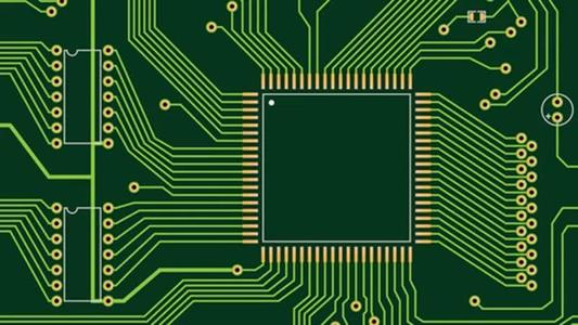
1. Capacitors generally use "C" and numbers in the circuit (such as a capacitor with a number 13 in C13). The capacitor is two pieces of gold Components composed of the membrane are tight and are separated by insulating materials in the middle. The characteristics of capacitors are mainly DC communication. The size of the capacitor capacity is to indicate the size of the energy storage. The obstacle of the capacitor to the communication signal is called the capacity of the capacity. The frequency of flow signal is related to electricity capacity. Rong resistance XC = 1/2πf C (f represents the frequency of the communication signal, C represents the capacitor capacity) The types of capacitors commonly used in the telephone are electrolytic capacitors, porcelain capacitors, patch capacitors, monopolic capacitors, 钽 capacitors and polyester capacitors wait. 2. Recognition method: The recognition method of capacitors is basically the same as the recognition method of resistance, a
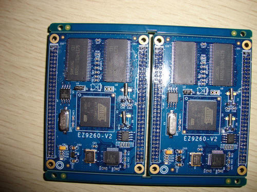
The resistance is represented by "R" in the circuit, such as: R1 represents a resistance number 1. The main role of resistance in the circuit is Diversion, current limit, pressure, bias, etc. 1. Parameter recognition: The unit of the resistance is Om (ω), the multiplier unit is: thousands of Euros (KΩ), Mago (MΩ), etc. Convert The method is: 1 trillion Euros = 1000,000 Euros = 1000000 Euros There are three types of parameter marking methods of the resistance, namely the direct marking method, the color standard method and the number of the number. A. The number of bidding methods is mainly used for small -volume circuits such as patch, such as: 472 represents 47 × 100Ω (ie 4.7K); 104 means 100K B. The color ring labeling method is used most most. Four -color ring resistance five -color ring resistance (precision resistance) 2. The relationship between the position and magnification of the resistance of the resistor is shown in the table below: Color valid digital multiplier
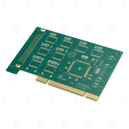
Base / thickness: FR-4 / 1.2mm Size: 140mm*159mm Minimum line width / line distance: 6mil / 6mil Minimum Pores: 0.4mm Surface treatment: Electro -plated File format: Gerber Category: Computer; Four Floor Base / thickness: FR-4 / 1.6mm Size: 294mm*200mm Minimum line width / line distance: 5mil / 5mil Minimum Pores: 0.3mm Surface treatment: tin spray (hot wind flat)
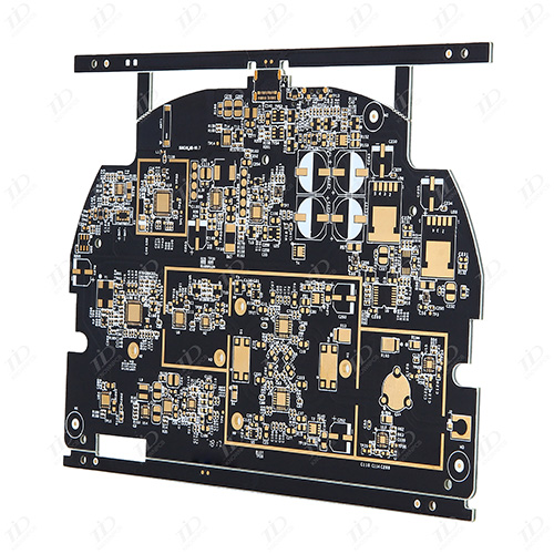
Generally speaking, the four -layer circuit board can be divided into top, bottom, and two middle layers. On the top and the bottom layer, the middle layer first uses Add Plane to add internal Plane1 and Internet Plane2 to the most power layer such as VCC and stratum (that is, the corresponding network labels are connected to the corresponding network label with ADD Plane Do not use Add Layer, this will increase the Midplayer, which is mainly used as a multi -layer signal line placement), so that Plnne1 and Plane2 are two layers of copper leather connected to the power VCC and ground GND. If there are multiple power supplies such as VCC2 or strata such as GND2, first use a thick wire or fill the Fill in Plane1 or Plane2 (at this time the bronze skin corresponding to the corresponding copper or the corresponding of Fill does not exist. You can clearly see the wire or obviously see the wire or you can clearly see the wire or the light or the light or Fill) The rough area of the power


Appointment Experience