Call Us Now! KnownPCB +86 755 2794 4155 KnownPCB sales@knownpcb.com
Shenzhen KNOWNPCB Technology Co., Ltd.
KnownPCBEN KnownPCBCN
KnownPCB
KnownPCB
About Us About Us

About Us

Home > 
  • About Us
  • >
  • News
  • How LED light work? Learn more about LED board

    How LED light work? Learn more about LED board

    Have you noticed that now more and more of our lighting is using led lighting.What is LED? Compared to the traditional light bulbs, LEDs have lower power consumption, longer lifetime and higher energy efficiency. In the PCB industry,when we say LED PCB, it refers to the pcb used for LED lighting, if you are looking for a suitable LED PCB for your lighting system, this article may bring you something. WHAT ARE LEDS COMPOSED OF?LED is an initial light-emitting diode that produces light when an electric current passes through. LEDs typically have negative and positive electrodes, which generate light in the visible light region.The LEDS are glued to the PCB by soldering process and have electrical connections for lighting.Since light-emitting diodes dissipate a lot of heat when they are in use, when you are designing LED, the metal core is usually the best choice for LED PCB, it is because that it dissipates heat more faster. Among them, the metal material aluminum is the most widely used

    Know Detail

    PCB Manufacturing Process.Process and function of intermediate pressure in circuit board production

    PCB Manufacturing Process.Process and function of intermediate pressure in circuit board production

    Mar 14,2024

        1. Check and remove the debris adhering to the semi-cured sheet;  2. Check the inner plate: and ensure that there is no debris adhering to it;  Our operators do a good job in the laminate positioning template (also known as the press template positioning pin) tooling, templates, and buffer paper before the plate.  Whether it is a senior circuit board manufacturer or our operator, according to the performance of the semi-cured sheet used, the relevant temperature setting size provisions: Tg<135t, the maximum temperature setting range is 160-185t; Tg>160t, the maximum temperature setting range is 170-205t.  The next step is the pressure of lamination: it squeezes the air between the plates and speeds up the flow of resin to fill the space between the shapes.  - Generally, the setting of pressure is divided into four stages:  ① Pre-pressure section: drive volatiles and residual gases, so that the layer is closely combined. Precompression is the key of lamination.  ② Medium pressure se

    Know Detail

    PCB high precision multi-layer circuit board production should have 6 characteristics

    PCB high precision multi-layer circuit board production should have 6 characteristics

    Mar 13,2024

        1, plate: multi-layer board are using Shengyi /KB A-grade copper-clad plate /PP, Sun/Guangxin ink. As a recognized leading enterprise in the copper clad plate industry, Shengyi board products are used in a large number of cutting-edge PCB factories around the world, and multi-layer board guarantees the excellent performance of PCB finished products from the source.  2, hole copper :PCB production has always strictly followed the IPC secondary standard, the thinnest hole copper of the finished product is greater than 20um, beyond the IPC -- level standard! Due to good plating uniformity and strong deep plating ability,PCB dares to ensure smooth and uniform copper plating of the hole and hole wall, and there is no serious uneven copper plating similar to "10 um somewhere, 30 um somewhere" If the user finds the thinnest copper of the finished hole is less than 20um,PCB promises a full refund;  3, line width and line distance: according to the control of 20% of the soil shipment, but t

    Know Detail

    Double-sided multilayer PCB circuit board assembly rules and skills

    Double-sided multilayer PCB circuit board assembly rules and skills

    Mar 13,2024

        1, PCB board width ≤260mm(SIEMENS line) or ≤300mm(FUJI line); If automatic dispensing is required, PCB board width × length ≤125 mm×180 mm.  2, PCB board appearance as close as possible to the conventional graphics, it is recommended to use 2*5, 3*3 board, can be assembled according to the thickness of the board;  3. The outer frame of the PCB assembly should adopt a closed-loop design to ensure that the assembly is fixed on the fixture without deformation.  4. The center distance between the small plates is controlled between 75 mm and 145 mm.  5. There can be no large components next to the connection point between the panel shape and the PCB internal small board, small board and small board, and the edge of the components and board should have a space greater than 0.5mm.  6, four positioning holes are opened at the four corners of the outer frame of the plate, plus the Mark point, the aperture is 4mm(±0.01mm); The strength of the hole should be moderate to ensure that it will no

    Know Detail

    PCB double-sided multilayer circuit board foaming ten reasons

    PCB double-sided multilayer circuit board foaming ten reasons

    Mar 13,2024

        1. Substrate processing problems, for some thinner pcb substrates, due to poor rigidity of the substrate, it is not appropriate to use the brush machine to brush the board, and attention should be paid to control the solid production and processing, so as not to cause the poor bonding force between the substrate copper foil and chemical copper caused by the board bubbling.  2. The surface of the plate in the machining (drilling, laminating, milling, etc.) process caused by oil, or other liquids contaminated with dust pollution surface, will cause the surface foaming phenomenon.  3. The copper brush plate is bad, the grinding plate pressure is too large before copper sinking, resulting in hole deformation, so that the hole foaming phenomenon will be caused in the process of copper plating and tin-spraying welding.  4. Washing problem, due to copper plating to go through a large number of chemical solution treatment, all kinds of acid and alkali inorganic, organic and other drug solv

    Know Detail

    PCB Surface Mount services.PCB four-layer board production process

    PCB Surface Mount services.PCB four-layer board production process

    Mar 12,2024

      Cutting: According to the requirements of engineering data MI, on the large sheet plate that meets the requirements, cut into small pieces of production plate. Small sheet material that meets customer requirements. Process: Large plate material - cut plate according to MI requirements - curium plate - beer rounded or edging - out of the plate.  Pressing: The pressing of the pcb four-layer board needs to go through two operations, first the inner two layers of the board after drilling, and then the outer layer and the inner layer are pressed again.  Drilling: According to the engineering data (customer data), drill out the desired aperture at the corresponding position on the sheet material that meets the required size. Process: Stack pin -- top board -- drilling -- bottom board -- inspection/repair.  Copper sinking: Copper sinking is the use of chemical methods on the insulation hole wall deposited on a thin layer of copper. Process: rough grinding -- hanging plate -- automatic coppe

    Know Detail

    Aluminum Substrates board.PCB six-layer circuit board impedance design should pay attention to what problems

    Aluminum Substrates board.PCB six-layer circuit board impedance design should pay attention to what problems

    Mar 12,2024

        1, the line width is wider than the fine line: because there is a fine line limit in the manufacturing process, the width is not limited. Adjusting the line width to adjust the impedance at a later stage and reach the limit can be cumbersome, which increases the cost or relaxes the impedance control.  2, there is an overall trend: there may be multiple impedance control targets in the design, so the overall size is too large or too small, and there is no need to be out of sync.  3, consider the residual copper rate and glue flow: when one or both sides of the prepreg are etched lines, during the pressing process, the glue will fill the etching gap, so the glue thickness time between the two layers is reduced. If the residual copper rate and glue flow rate are not calculated correctly, and the dielectric coefficient of the new material is not consistent with the nominal value, signal integrity problems may occur.  4, specify the glass cloth and glue content: different glue content o

    Know Detail

    multilayer pcb manufacture.What is the purpose of PCB drilling

    multilayer pcb manufacture.What is the purpose of PCB drilling

    Mar 12,2024

        Through hole (VIA), this is a common hole used for conducting or connecting copper foil lines between conductive patterns in different layers of the circuit board. Such as (e.g., blind holes, buried holes), but can not insert the component lead leg or other reinforcement material copper plated holes. Because the PCB is formed by the accumulation of many copper foil layers, each layer of copper foil will be covered with a layer of insulation layer, so that the copper foil layer can not communicate with each other, and the link of its signal depends on the through hole (via), so there is the title of the Chinese through hole.  The characteristic is: in order to meet the needs of customers, the through hole of the circuit board must be strengthened, so that in changing the traditional aluminum plug process, the circuit board surface welding and plug hole are completed with white mesh, so that the production is stable, the quality is reliable, and the use is more perfect. The through h

    Know Detail

    PCBA Assembly Manufacturer.Reasons for excessive consumption of copper-plated copper balls in circuit board production

    PCBA Assembly Manufacturer.Reasons for excessive consumption of copper-plated copper balls in circuit board production

    Mar 11,2024

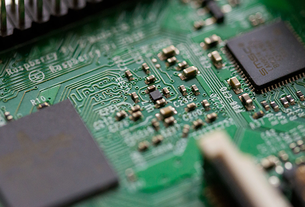
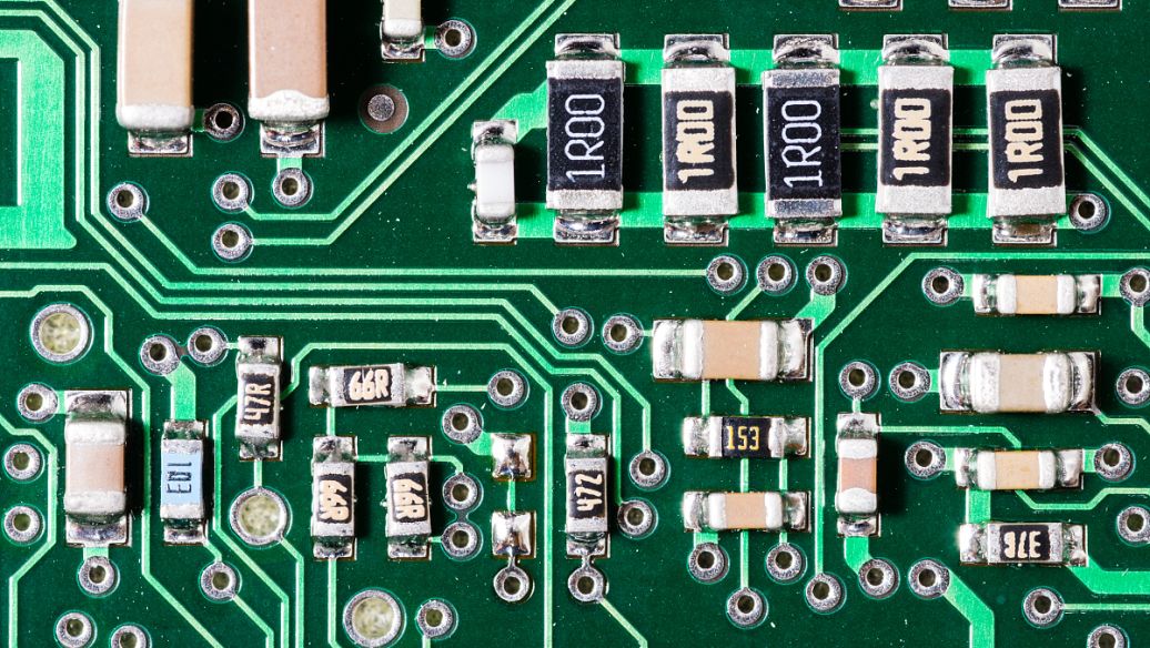
       The content of copper sulfate in each analysis in the production is low, originally divided once a week, and now in the case of excessive consumption, it is divided every day, and copper sulfate has decreased every day, originally controlled in 60-80g/L, but just added the day before, and the next day less 6-7G, I wonder why copper sulfate consumption is so large.  Subsequently, according to the production volume to follow up, according to the production capacity of each shift is about 30 square meters, about 60 square meters a day, the copper consumption is about 21KG a day, a large slot of copper ball is about 1400KG, according to the production needs to consume 21KG a day, so, according to the theory, the copper ball must be added every week 147KG. After two weeks of observation, the copper ball was not replenished in time in production, and it must be replenished every week, but now it is only replenished once every two weeks. After analysis and observation, it is found that the

    Know Detail
  • 第一页
  • <
  • 4
  • 5
  • 6
  • 7
  • 8
  • 9
  • 10
  • 11
  • 12
  • >
  • 最后一页
  • ogo

    Appointment Experience

    X