Call Us Now! KnownPCB +86 755 2794 4155 KnownPCB sales@knownpcb.com
Shenzhen KNOWNPCB Technology Co., Ltd.
KnownPCBEN KnownPCBCN
KnownPCB
KnownPCB
About Us About Us

About Us

Home > 
  • About Us
  • >
  • News
  • How LED light work? Learn more about LED board

    How LED light work? Learn more about LED board

    Have you noticed that now more and more of our lighting is using led lighting.What is LED? Compared to the traditional light bulbs, LEDs have lower power consumption, longer lifetime and higher energy efficiency. In the PCB industry,when we say LED PCB, it refers to the pcb used for LED lighting, if you are looking for a suitable LED PCB for your lighting system, this article may bring you something. WHAT ARE LEDS COMPOSED OF?LED is an initial light-emitting diode that produces light when an electric current passes through. LEDs typically have negative and positive electrodes, which generate light in the visible light region.The LEDS are glued to the PCB by soldering process and have electrical connections for lighting.Since light-emitting diodes dissipate a lot of heat when they are in use, when you are designing LED, the metal core is usually the best choice for LED PCB, it is because that it dissipates heat more faster. Among them, the metal material aluminum is the most widely used

    Know Detail

    The method of improving the yield of fine line products

    The method of improving the yield of fine line products

    Mar 21,2024

      Step 1 Drill holes  The design of the through hole aperture below 8mil, the hole spacing is close, plus each board about 500,000 to 1.2 million blind holes, the hole deviation and plugging of the through hole, and the perforation of the perforation will affect the PCB yield. Drilling machine needs to be maintained according to the regulations, the use of appropriate aluminum sheet and drill nozzle, in the production of new materials engineers to confirm the rationality of the operation parameters: number of sheets, tool parameters, etc. The amount of dust suction of the drilling machine needs to meet the standard, and the drilling needle has space for debris removal is also crucial. The pass shape and aperture, dielectric thickness, material and laser energy of the laser are very important, and it is necessary to set the best operating conditions.  Step 2: Electroplating  Electroplated copper carries the functions of current conduction and signal transmission, and the electroplating

    Know Detail

    Nelco PCB Manufacturing.Plating technique of through holes with high aspect ratio of plating holes

    Nelco PCB Manufacturing.Plating technique of through holes with high aspect ratio of plating holes

    Mar 20,2024

        Printed circuit board manufacturing industry more and more need high aspect ratio, small hole printed circuit board plating process. It is the driving force to promote the development of high-level multi-layer printed circuit board manufacturing technology. Because of the reliability of the hole coating, it plays a key role in the use of printed circuit boards. How to ensure the problem of high aspect ratio deep hole plating is the scientific and technological task of all printed circuit workers, and it is the most important problem that must be faced. To this end, many research departments began to carry out planned research and development. There are many methods reported from the current scientific and technological data, including pulse plating technology, chemical vapor deposition technology, solution impact plating technology, full electroless copper plating technology and improved (high acid and low copper) air stirring technology. This part of the technology is introduced a

    Know Detail

    Flexible PCB Prototypes.PCB film deformation correction process

    Flexible PCB Prototypes.PCB film deformation correction process

    Mar 20,2024

        1, in the case of mastering the operation technology of the digital programming instrument, first load the film and the drilling test plate, measure the length and width of the two deformation, in the digital programming instrument according to the size of the deformation of the hole to lengthen or shorten the hole, with the drilling test plate after lengthening or shortening the hole to match the deformed film, eliminating the tedious work of splicing the film, to ensure the integrity and accuracy of the graph. This method is called "changing hole position method".  2, in view of the physical phenomenon that the negative changes with the change of ambient temperature and humidity, the negative in the sealed bag is taken out before the copy of the negative, and the working environment conditions are hung for 4-8 hours, so that the negative is deformed before the copy, so that the deformation of the negative after the copy is very small, called this method "hanging method".  3. For

    Know Detail

    PCB circuit board design.PCB related methods precautions

    PCB circuit board design.PCB related methods precautions

    Mar 20,2024

        1. Splicing method:  Applicable: The line is not too dense, the film deformation of each layer is inconsistent; It is especially suitable for the deformation of solder resistance plate and multilayer plate power formation plate.  Not applicable: film with high wire density, line width and spacing less than 0.2mm;  Note: When splicing, the wire should be damaged as little as possible, and the welding pad should not be damaged. When splicing copy after revision, attention should be paid to the correctness of the connection relationship.  2, change the hole position method:  Application: All layers of film deformation is consistent. This method also applies to film with dense lines;  Not applicable: film deformation is not uniform, local deformation is particularly serious.  Note: After using the programmer to lengthen or shorten the hole position, the out-of-tolerance hole position should be reset.  3, hanging method:  Applicable; Film that has not been deformed and is protected from

    Know Detail

    custom pcb circuit board.PCB production equipment

    custom pcb circuit board.PCB production equipment

    Mar 19,2024

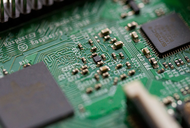
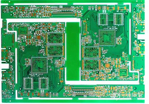
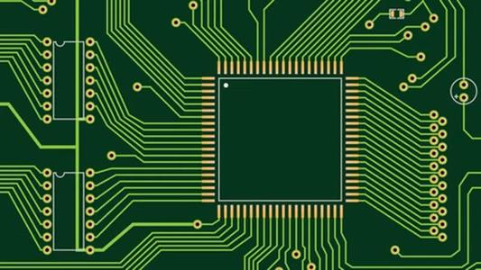
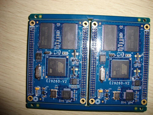
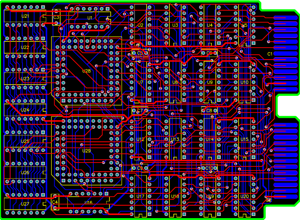
        1, engineering production -- light painting machine, film exposure machine  2, opening - opening machine, baking plate oven  3, laminating - brown production line, laminating machine, grinding machine  4, drilling -- CNC drilling machine  5, grinding board -- grinding machine  6, Metallized hole (PTH)-- chemical copper production line (copper wire)  7, graphics transfer - film machine, UV exposure machine or LDI  8, graphic plating - plating production line  9, dry (wet) film - film production line  10, graphic etching ---- etching production line  11, welding resistance layer production -- screen printing machine, UV exposure machine or LDI  12, baking and curing ---- oven, tunnel oven  13, surface treatment --OSP production line or chemical nickel gold line, chemical nickel palladium gold line  14, molding -- punching machine or CNC gong machine, cutting machine  15. Test -- Electric Measuring machine, AOI, 3DAOI.  4, the plate is scratched during the transfer process:  a, the ha

    Know Detail

    quick-turn PCB prototype.Circuit board surface treatment process

    quick-turn PCB prototype.Circuit board surface treatment process

    Mar 19,2024

        1, hot air smoothing (spray tin)  Hot air smoothing, also known as hot air solder smoothing (commonly known as spray tin), it is the process of coating molten tin (lead) solder on the surface of the PCB and heating compressed air to smooth (blow), so that it forms a coating layer that is resistant to copper oxidation and can provide good solderability. During hot air conditioning, a copper-tin metal intermetallic compound is formed at the joint of solder and copper. PCB for hot air finishing usually to sink in the molten solder; The air knife blows out the liquid solder before it solidifies; The air knife minimizes the meniscus of solder on the copper surface and prevents solder bridging.  2, organic weldability protectant (OSP)  OSP is a process for printed circuit board (PCB) copper foil surface treatment in accordance with the requirements of the RoHS directive. OSP is short for Organic Solderability Preservatives, also known as organic solderability preservatives, also known as

    Know Detail

    PCB open circuit reasons and improvement methods

    PCB open circuit reasons and improvement methods

    Mar 19,2024

        Improvement method:  1, the copper clad plate in the warehouse before IQC must be random inspection, check whether the surface of the board scratches the substrate phenomenon, if there should be timely contact with the supplier, according to the actual situation, make appropriate treatment.  2, the copper clad plate is scratched during the opening process, the main reason is that there are hard objects on the surface of the opening machine, and the friction between the copper clad plate and the objects causes the copper foil scratch to form the phenomenon of exposing the substrate, so the table must be carefully cleaned before the opening of the material to ensure that the table is smooth and there is no hard objects.  3, the copper clad plate is scratched by the drill when drilling, the main reason is that the spindle clip is worn, or the debris in the clip is not clean, the drill is not firmly grasped, the drill does not go to the top, the length of the drill is slightly longer t

    Know Detail

    RO4000 Laminates RO4350B Cavity Opening Board

    RO4000 Laminates RO4350B Cavity Opening Board

    Mar 18,2024

    RO4000 Laminates RO4350B Cavity Opening BoardRo4350B material, cavity opening at L1-L2&L6-L5, 4mil bonding pad.Details: Cavity from Top Layer to L2. L2 has exposed pads with ENEPlG Plating for Wire Bonding.Cavity from Bottom Layer to L5. L5 has exposed pads with ENEPIG Plating for Wire Bonding.The 2 cavities are symmetric with each other.

    Know Detail
  • <
  • 1
  • 2
  • 3
  • 4
  • 5
  • 6
  • 7
  • 8
  • 9
  • >
  • 最后一页
  • ogo

    Appointment Experience

    X