Call Us Now! KnownPCB +86 755 2794 4155 KnownPCB sales@knownpcb.com
Shenzhen KNOWNPCB Technology Co., Ltd.
KnownPCBEN KnownPCBCN
KnownPCB
KnownPCB
About Us About Us

About Us

Home > 
  • About Us
  • >
  • News
  • How LED light work? Learn more about LED board

    How LED light work? Learn more about LED board

    Have you noticed that now more and more of our lighting is using led lighting.What is LED? Compared to the traditional light bulbs, LEDs have lower power consumption, longer lifetime and higher energy efficiency. In the PCB industry,when we say LED PCB, it refers to the pcb used for LED lighting, if you are looking for a suitable LED PCB for your lighting system, this article may bring you something. WHAT ARE LEDS COMPOSED OF?LED is an initial light-emitting diode that produces light when an electric current passes through. LEDs typically have negative and positive electrodes, which generate light in the visible light region.The LEDS are glued to the PCB by soldering process and have electrical connections for lighting.Since light-emitting diodes dissipate a lot of heat when they are in use, when you are designing LED, the metal core is usually the best choice for LED PCB, it is because that it dissipates heat more faster. Among them, the metal material aluminum is the most widely used

    Know Detail

    multilayer pcb manufacture.PCB industry shift accelerates

    multilayer pcb manufacture.PCB industry shift accelerates

    Apr 11,2024

      The general trend of industrial eastward movement, the mainland region outshines. The focus of the PCB industry continues to shift to the Asian region, and the capacity of the Asian region has further transferred to the mainland, forming a new industrial pattern.  Applications such as data centers increase the demand for HDI, and the future space for FPC is broad. Data centers are developing towards the characteristics of high speed, large capacity, cloud computing, and high performance, and the construction demand is surging, among which the demand for servers will also pull up the overall demand for HDI. The popularity of mobile electronic products such as smartphones will also drive the demand for FPC boards. In the trend of intelligent and thin mobile electronic products, the advantages of light weight, thin thickness and bending resistance of FPC will be conducive to its wide application. The demand for FPC in the display module, touch module, fingerprint recognition module, sid

    Know Detail

    Layout and procedure of circuit board

    Layout and procedure of circuit board

    Apr 10,2024

        1) Single panel: This type of panel is usually used in the case of lower cost requirements. In layout design, sometimes components are needed or jumper wires are used to skip the circuit board's wiring. If there are too many, you should consider using dual panels.  2) Dual panel: Dual panel can be used or not to use PTH. Because PTH boards are expensive, they are only used when the complexity and density of the circuit require them.  In general, the choice between a single panel or a dual panel must meet the most efficient cost utilization. As a rule of thumb, the cost of a double-sided printed board with plated through holes is 5-10 times that of a single panel. Similarly, the cost of assembling components is also an important aspect to consider, the cost of assembling a single-sided printed circuit board component (manual) is about 25%-50% of the cost of the circuit board, and the cost of assembling a double-sided printed circuit board component with PTH is 15%-30% of its cost.  

    Know Detail

    nspection and related technology of assembled circuit board

    nspection and related technology of assembled circuit board

    Apr 10,2024

        Automatic optical inspection (AOI) systems are commonly used to test the inner layer before the formation of layers. After stratification, X-ray systems monitor alignment accuracy and minor defects; A scanning laser system provides a way to detect the layer before reflow. These systems, along with line visual inspection technology and component integrity testing for automatically placed components, help ensure the reliability of the final assembly and welded plates.  However, even if these efforts minimize defects, the final inspection of the assembled printed circuit board is still required, which is perhaps the most important, as it is the final unit for product and overall process evaluation.  The final inspection of the assembled PCB board may be done by an active method or by an automated system, and often both methods are used together. Manual "means that an operator uses optical instruments to visually inspect the board and make a correct judgment about the gap. Automated sy

    Know Detail

    Fabrication circuit boards.nspection and related technology of assembled circuit board

    Fabrication circuit boards.nspection and related technology of assembled circuit board

    Apr 09,2024

        Automatic optical inspection (AOI) systems are commonly used to test the inner layer before the formation of layers. After stratification, X-ray systems monitor alignment accuracy and minor defects; A scanning laser system provides a way to detect the layer before reflow. These systems, along with line visual inspection technology and component integrity testing for automatically placed components, help ensure the reliability of the final assembly and welded plates.  However, even if these efforts minimize defects, the final inspection of the assembled printed circuit board is still required, which is perhaps the most important, as it is the final unit for product and overall process evaluation.  The final inspection of the assembled PCB board may be done by an active method or by an automated system, and often both methods are used together. Manual "means that an operator uses optical instruments to visually inspect the board and make a correct judgment about the gap. Automated sy

    Know Detail

    The difficulty encountered in the manufacture of aluminum substrate

    The difficulty encountered in the manufacture of aluminum substrate

    Apr 08,2024

        1, engineering design line width compensation: due to the thick copper, the line width must be compensated, otherwise the line width is too poor after etching, the customer is not accepted, the line width compensation value must experience stacking.  2, the uniformity of print resistance welding: due to the ultra-normal copper thickness of the line after graphic etching, print resistance welding is very difficult, skip printing, too thick and too thin customers do not bear. How to print this layer of green oil is also one of the difficulties.  3. Etching: The line width after etching must meet the needs of customer drawings. The residual copper is not allowed, nor can the knife be scraped away, the knife will scratch the insulation layer, resulting in sparks and leakage in the voltage test.  4, mechanical processing: aluminum substrate drilling can be, but the drilling hole inside the hole edge is not allowed to have any burrs, which will affect the pressure test. Milling shape is

    Know Detail

    Introduction of multilayer high frequency circuit board.hot pot table 10 seats

    Introduction of multilayer high frequency circuit board.hot pot table 10 seats

    Apr 03,2024

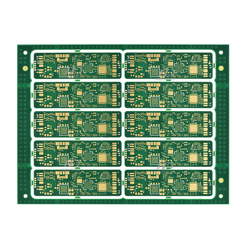
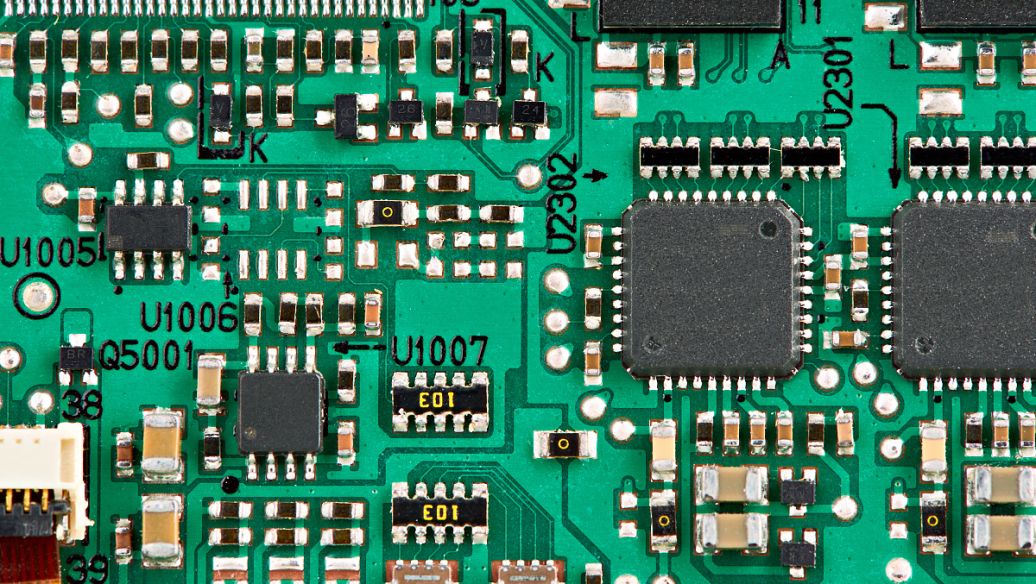
        1. It has the characteristics of small signal transmission loss, short transmission delay time and small signal transmission distortion.  2. Excellent dielectric properties (mainly: low relative dielectric constant Dk, low dielectric loss factor Df). Moreover, this dielectric property (Dk, Df) can maintain its stability under environmental changes in frequency, humidity, and temperature.  3. High precision control with characteristic impedance (Zo).  4. Excellent heat resistance (Tg), processability and adaptability.  Based on the above characteristics, high-frequency PCB boards are widely used in wireless antennas, base station receiving antennas, power amplifiers, components (shitters, confluence, filters), radar systems, navigation systems and other communication equipment.  Multi-layer high frequency plate design, based on cost savings, improving bending strength, electromagnetic interference control and other factors, often in the form of hybrid plate, called high frequency hy

    Know Detail

    heavy copper PCB manufacturer.Circuit board welding process and related requirements

    heavy copper PCB manufacturer.Circuit board welding process and related requirements

    Apr 03,2024

        1. Welding materials  1) The solder usually adopts Sn60 or Sn63 solder that meets the general standard of the United States, or adopts HL-SnPb39 type tin lead solder.  2) The flux can usually be rosin flux or water-soluble flux, the latter is generally only used for wave soldering.  3) The cleaning agent should ensure that the PCB board is non-corrosive and pollution-free, generally using anhydrous ethanol (industrial alcohol), trichlorotrifluoroethane, isopropanol (IPA), aviation washing gasoline and deionized water and other cleaning agents for cleaning. The specific cleaning agent used should be selected according to the process requirements.  2. Welding tools and equipment  1) The reasonable selection of the power and type of soldering iron has a direct relationship to improving welding quality and efficiency. It is recommended to use low-voltage temperature-controlled electric soldering iron, the soldering iron head can be nickel plated, iron plated or copper material, the sha

    Know Detail

    Fast turn PCB prototype board.Circuit board printed wire width selection basis

    Fast turn PCB prototype board.Circuit board printed wire width selection basis

    Apr 02,2024

        The minimum width of the printed wire is related to the size of the current flowing through the wire: the line width is too small, the resistance of the just-printed wire is large, the voltage drop on the line is large, affecting the performance of the circuit, the line width is too wide, the wiring density is not high, the board area increases, in addition to increasing the cost, it is not conducive to miniaturization. If the current load is calculated at 20A/ mm2, when the thickness of the copper clad foil is 0.5MM,(generally so much,) the current load of 1MM(about 40MIL) line width is 1A,  Therefore, the line width of 1--2.54MM(40--100MIL) can meet the general application requirements, the ground wire and power supply on the high-power equipment board, according to the power size, can be appropriately increased line width, and in the low-power digital circuit, in order to improve the wiring density, the minimum line width of 0.254--1.27MM(10--15MIL) can be full Full. Same circui

    Know Detail
  • <
  • 1
  • 2
  • 3
  • 4
  • 5
  • 6
  • 7
  • >
  • 最后一页
  • ogo

    Appointment Experience

    X