 +86 755 2794 4155
  sales@knownpcb.com
-
Shenzhen KNOWNPCB Technology Co., Ltd.
 +86 755 2794 4155
  sales@knownpcb.com
With the continuous expansion of the company's scale, the original company's website has been far from enough...
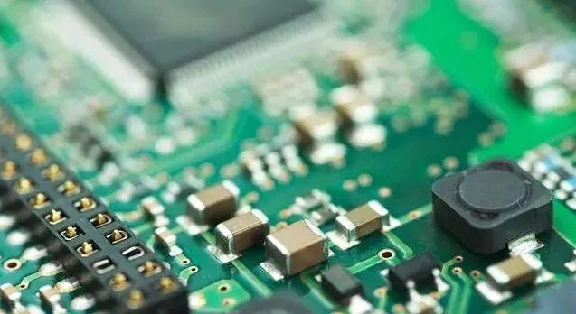
HDI (High Density Interconnect Board) is a compact circuit board designed specifically for small capacity users. Compared to ordinary PCBs, the most significant feature of HDI is its high wiring density, which is mainly reflected in the following four aspects.
1、HDI is smaller and lighter
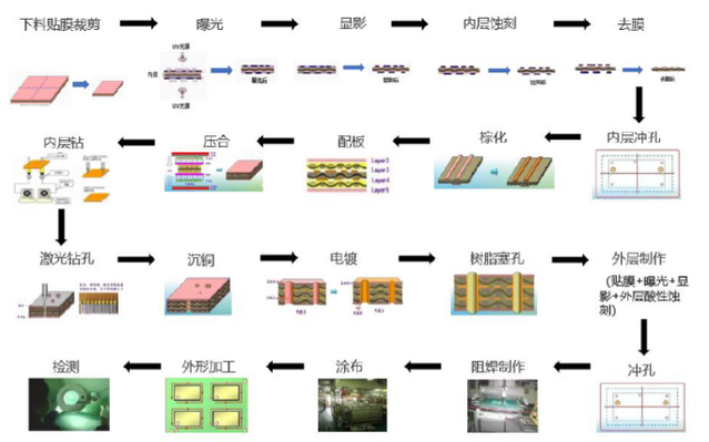
The HDI board is made of the traditional double-sided board as the core board through continuous lamination. This kind of circuit board made by continuous layering is also called build-up multilayer board (Build-up Multilayer, BUM). Compared with traditional circuit boards, HDI circuit boards have the advantages of "light, thin, short, and small".
The electrical interconnection between HDI board layers is realized through conductive through holes, buried holes and blind holes. Its structure is different from ordinary multilayer circuit boards. A large number of micro-buried blind holes are used in HDI boards. HDI uses laser direct drilling, while standard PCB usually uses mechanical drilling, so the layer count and aspect ratio tend to be reduced.
2、HDI production process

The high density of HDI boards is mainly reflected in the density of holes, lines, pads, and interlayer thickness.
● Micro guide hole: HDI board contains micro guide hole design such as blind hole, which is mainly manifested in the micro hole forming technology with a diameter of less than 150um and the high requirements in terms of cost, production efficiency and hole position precision control. There are only through holes in traditional multilayer circuit boards without tiny buried blind holes
● Refinement of line width and line spacing: it is mainly manifested in increasingly stringent requirements for wire defects and wire surface roughness. Generally, the line width and line spacing do not exceed 76.2um
● High pad density: the density of solder joints is greater than 50 per square centimeter
● Thinning of dielectric thickness: It is mainly manifested in the trend of interlayer dielectric thickness to 80um and below, and the requirements for thickness uniformity are becoming more and more stringent, especially for high-density boards and packaging substrates with characteristic impedance control.
3、HDI boards with better electrical properties

HDI not only enables more miniaturized end product designs, but also meets higher standards of electronic performance and efficiency at the same time.
The increased interconnect density of HDI allows for enhanced signal strength and increased reliability. In addition, HDI boards have better improvements in radio frequency interference, electromagnetic wave interference, electrostatic discharge, and heat conduction. HDI also adopts all-digital signal process control (DSP) technology and a number of patented technologies, which have full-range adaptive load capacity and strong short-term overload capacity.
4、HDI boards with very high requirement for buried vias filled vias.
As can be seen from the above, HDI is superior to ordinary PCB in both volume and electrical performance. Every coin has two sides, the other side of HDI is as a high-end PCB manufacturing, its manufacturing threshold and process difficulty are much higher than ordinary PCB, the production should pay attention to more problems - especially the buried vifilled vias.
At present, the core pain point and difficulty of HDI manufacturing is buried hole plugging. If the HDI buried hole plug hole is not done well, there will be major quality problems, including uneven board edges, uneven dielectric thickness, and pitted pads.
● If the surface of the board is uneven and the line is not straight, it will cause beach phenomenon in the depression, which will cause defects such as line gaps and broken lines
● The characteristic impedance will also fluctuate due to the uneven dielectric thickness, resulting in signal instability
● The unevenness of the pad leads to poor quality of subsequent packaging and consequential losses of components
Therefore,not all board factories have the ability and strength to do a good job in HDI. Guangke HDI already has its own complete system and spends a lot of money to purchase advanced equipment. All quality acceptance standards have always adopted IPC2 standards to ensure high reliability.
Read recommendations:
FR4 Printed Circuit Board Assembly


Appointment Experience