
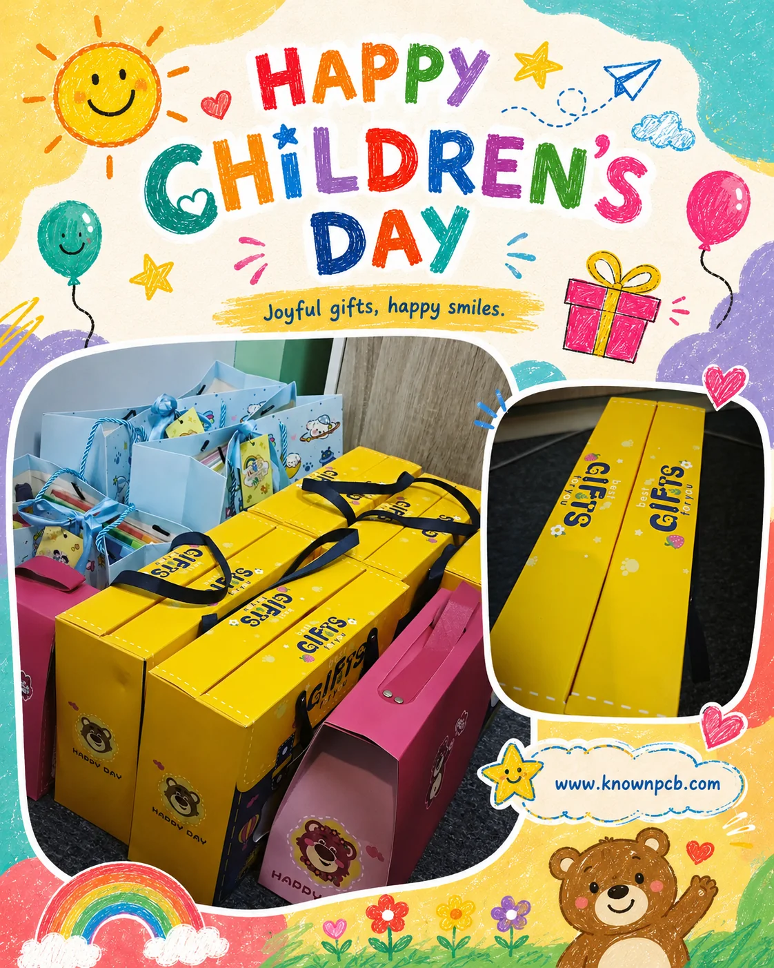
Children’s Day · Employee Family Care Celebrating Children’s Day with Our Employees and Their FamiliesA small gift can bring a big smile. This Children’s Day, KNOWNPCB shares wa...
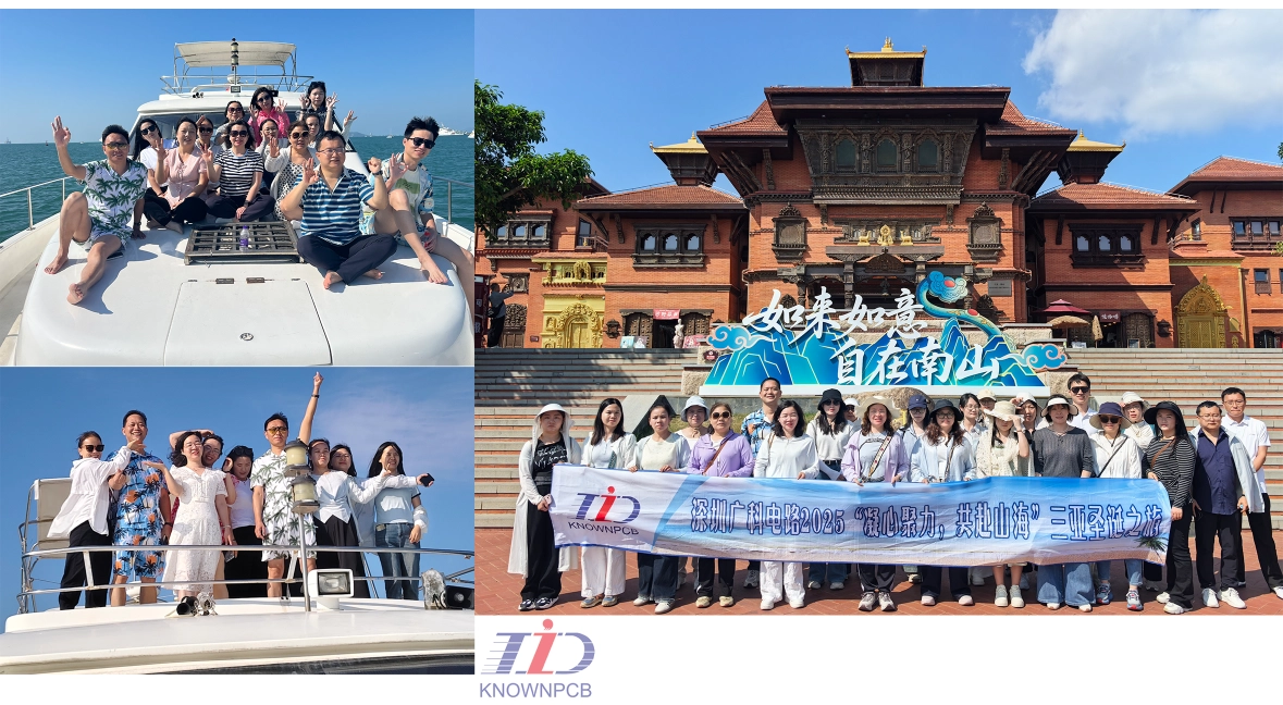
Team Building Sanya Retreat PCB Manufacturing Client Service At KnownPCB, quality comes from people. Our Sanya team retreat strengthened collaboration, trust, and energy across depa...
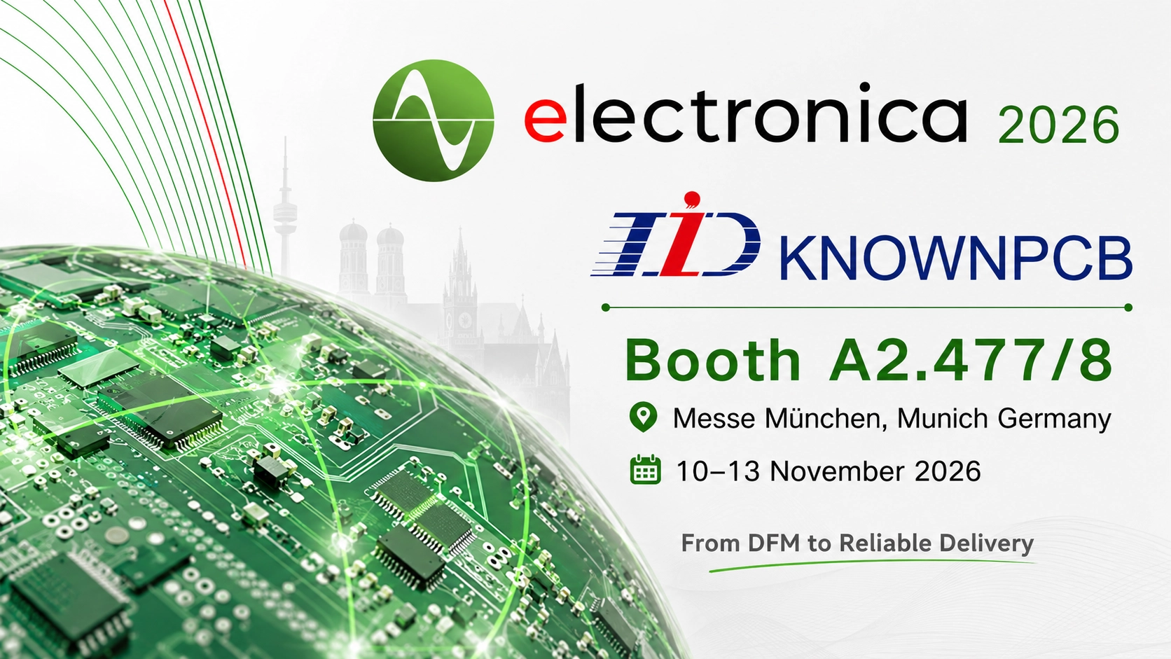
Meet KnownPCB at electronica 2026: From DFM to Reliable DeliveryDate: November 10–13, 2026 Venue: Messe München Booth: A2.477/8 KnownPCB will attend electronica 2026 at ...
As AI server constantly keep developing, the printed circuit board (PCB) industry is entering a new stage. Recently, based on updates from a leading PCB manufacturer in China, KnownPCB notices that ...
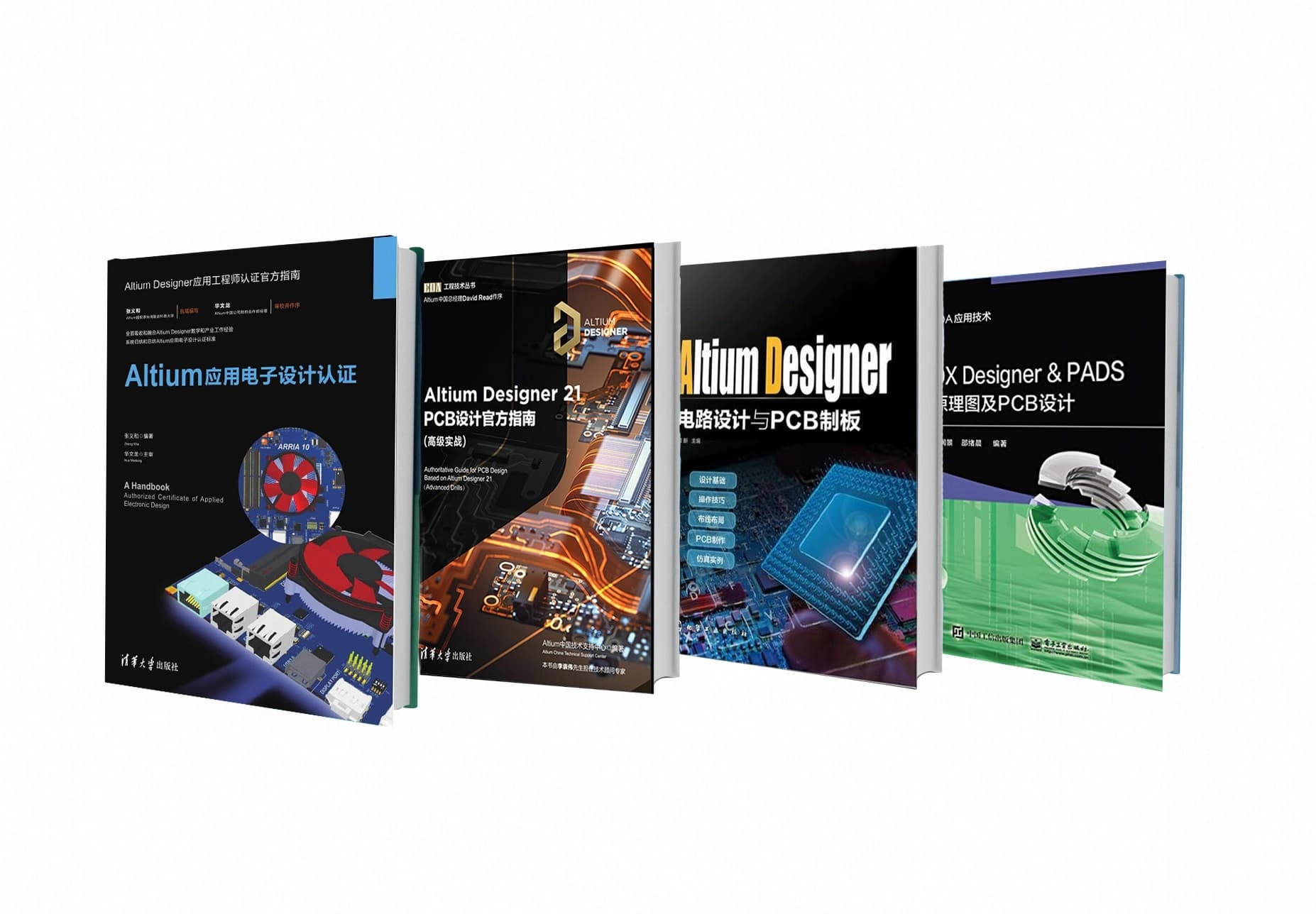 | Download our design guidesfor better PCB designing and manufacturing These are some of the design guides designers and engineersdownload the most:
|
Proven by 7 industries, 4000+ customer projects
Please contact us at sales@knownpcb.com, ask for engineering support here or use the form below to reach out to KnownPCB | Get In Touch Today |

