Prototype PCB Board Assembly Factory in China | Low MOQOne Supplier for SMT, THT, DFM, and Production Builds
We provide end-to-end PCB assembly services, SMT, THT, testing, and full engineering review built for prototype PCB assembly, NPI builds, and reliable low-to-mid volume production. Request a Fast PCBA Quote Upload Your Gerber & BOM Files |

Key Capabilities | |
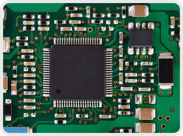
DFM/DFA review To prevent assembly defects in HDI, fine-pitch, and high-density layouts. | Component sourcing & BOM validation With part alternates to avoid shortages. |
SMT assembly for complex packages Including BGA, QFN, LGA, CSP, and 01005 passives. | Reflow profiling & thermal control Optimized for heavy-copper, thin-core, and mixed-layer PCBs. |
THT and selective soldering For power devices, high-current connectors, and mixed-technology builds. | SPI/AOI/X-ray inspection For solder joint quality, BGA voiding detection, and assembly reliability. |
Electrical testing & functional checks To validate signal integrity and final board performance. |
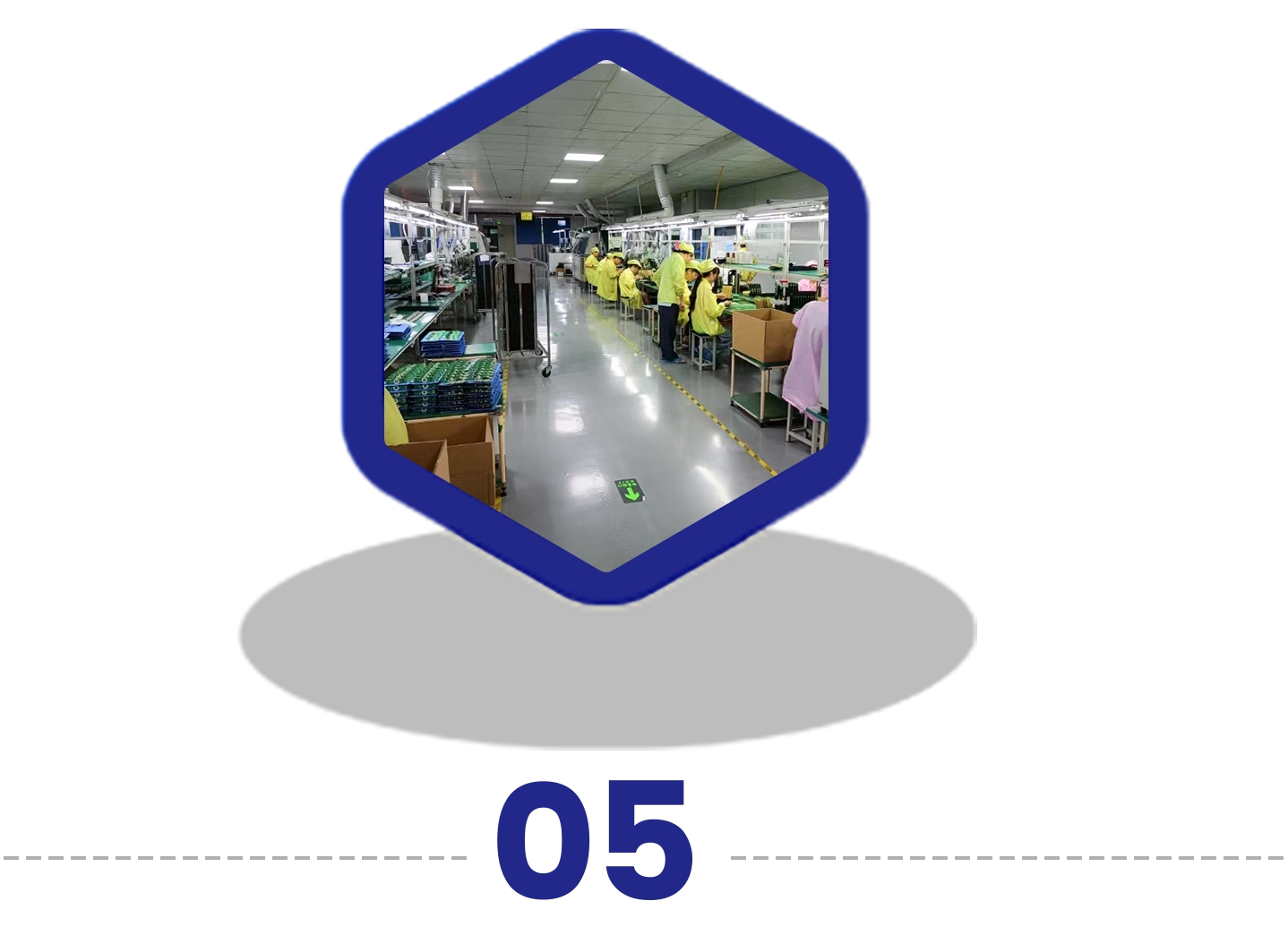
Support for prototype, NPI, low-volume, and mass-production PCBA builds.
Capable of handling rigid, flex, and rigid-flex PCBs with single-sided or double-sided SMT placement.
Submit Your Files for a Free DFM Review
| Item | Sub-item | Standard Capability | Limited Capability | Remark |
|---|---|---|---|---|
| SMT Process | PCB - Min Size | L≥30mm, W≥30mm | L<30mm, W<30mm | BOT, TOP sides components, Fiducial Mark should be ≥3mm from the board edge |
| PCB - Max Size | L≤650mm, W≤400mm | L:800-650mm, W:400-450mm | ||
| PCB - Component thickness(T) | 0.5mm ≤ T ≤ 3mm | T < 0.5mm, T > 3mm | ||
| Component size - Min Package | 0201 (0.6mm*0.3mm) | 01005 (0.3mm*0.2mm) | ||
| QFP, QFN, SOP, SOJ - Min Pin distance | 0.4mm | 0.3mm ≤ Pitch < 0.4mm | ||
| CSP, BGA - Min Pitch distance | 0.4mm | 0.3mm ≤ Pitch < 0.4mm | ||
| DIP Process (Wave soldering) | PCB Size - Min Size | L≥30mm, W≥30mm | L<30mm | |
| PCB Size - Max Size | L≤650mm, W≤400mm | L:800-650mm, W:400-450mm | ||
| PCB Size - Thinnest Size | 0.4mm | T < 0.4mm | ||
| PCB Size - Thickest Size | 5mm | T > 5mm | ||
| Conformal Coating Process | Temperature range | -30℃ ≤ T ≤ 120℃ | -50℃ ≤ T ≤ 150℃ | |
| Coating thickness | 20um ≤ T ≤ 35um | 35um ≤ T ≤ 60um |
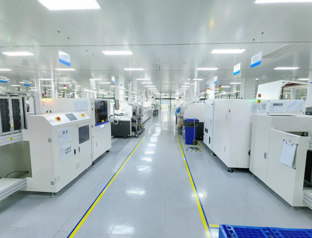
High-performance SMT lines equipped with automated stencil printers, advanced pick-and-place platforms, multi-zone reflow ovens, wave and selective soldering systems, and inline SPI/AOI/X-ray inspection.
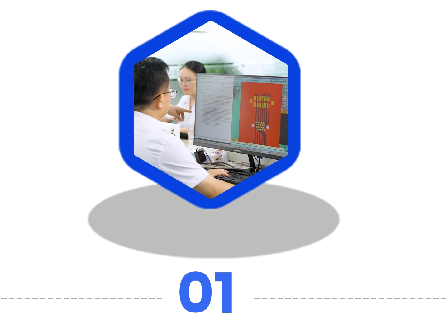 Design & File Review (DFA)Process Description Validate Gerber/BOM accuracy, ensure manufacturability, and identify layout risks before production begins. Key Technical Requirements Correct footprints; spacing & clearance; thermal relief design; BOM validation; DFM/DFA compliance. | 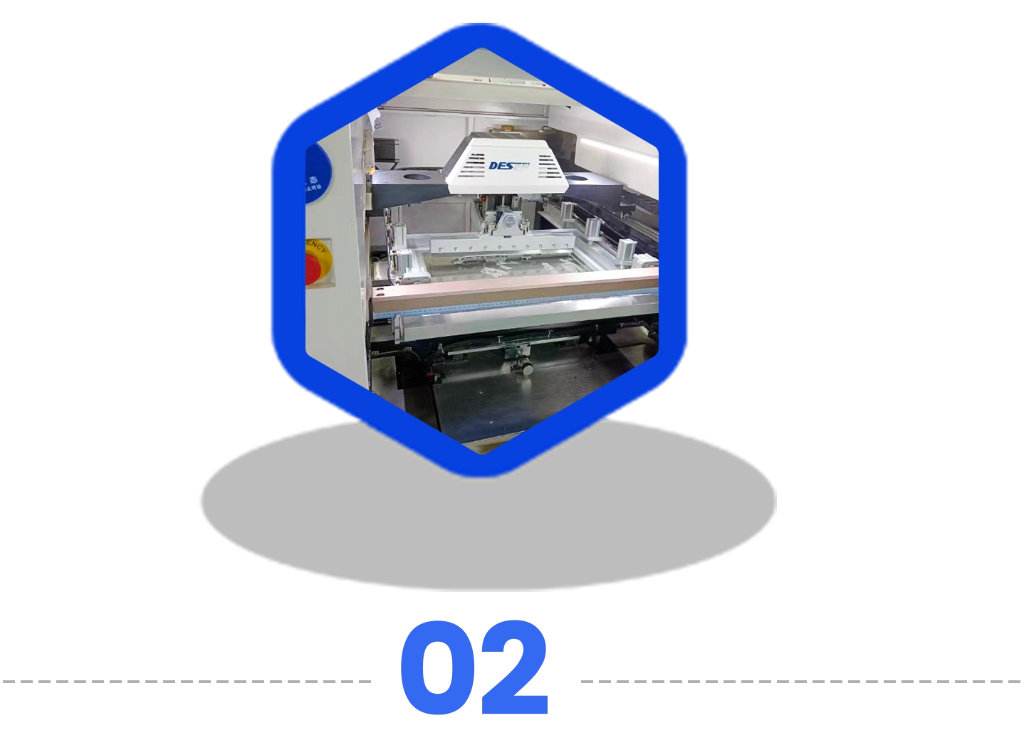 Solder Paste PrintingProcess Description Apply solder paste precisely to SMT pads using stencil alignment, ensuring consistent volume and clean pad definition. Key Technical Requirements Laser-cut stencil accuracy; controlled paste viscosity; | 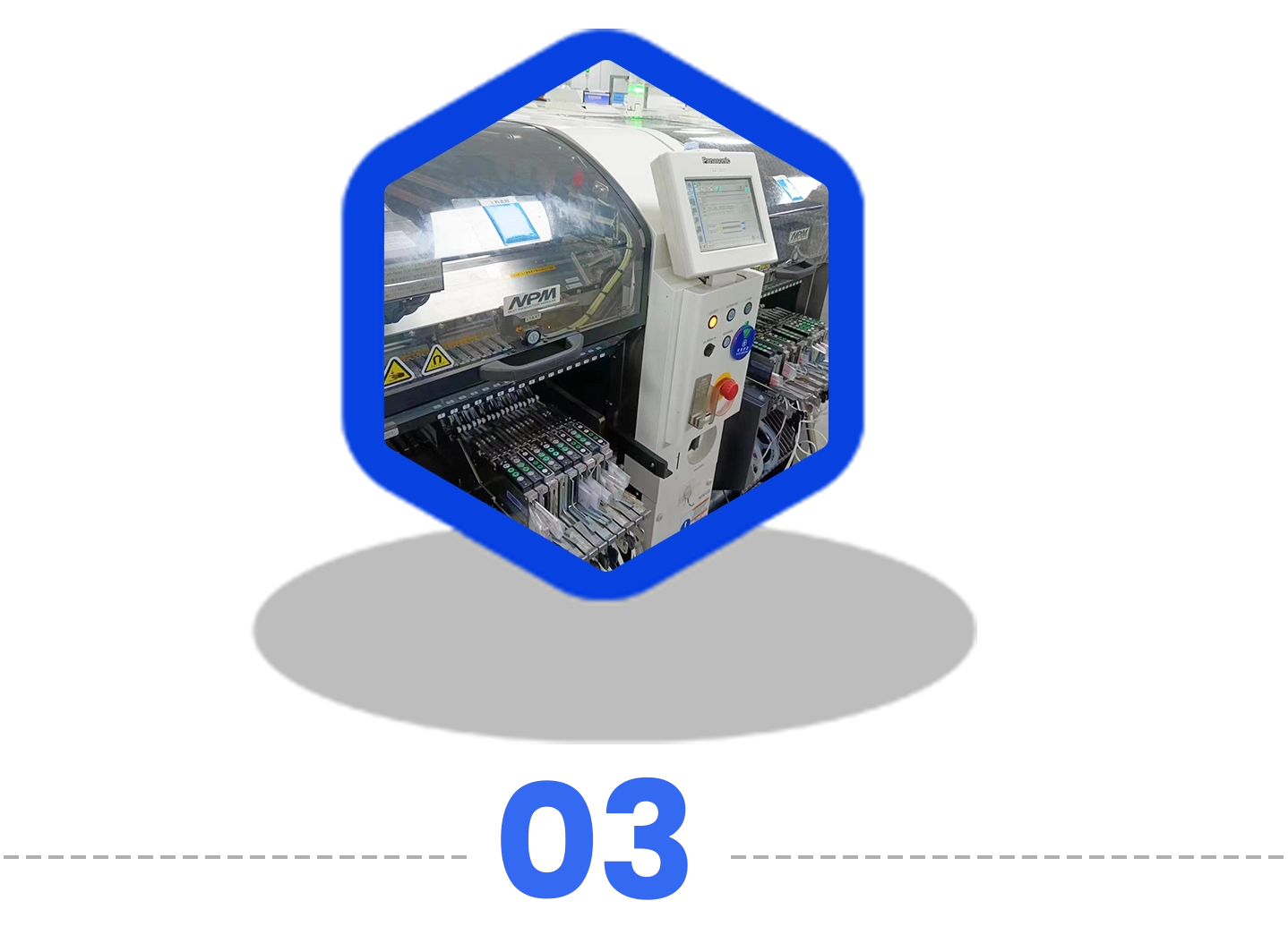 SMT Component PlacementProcess Description Place SMD components at high speed with vision alignment to ensure accuracy for fine-pitch and miniature packages. Key Technical Requirements Optical centering; feeder calibration; fine-pitch handling (BGA/QFN/01005); placement accuracy control. | 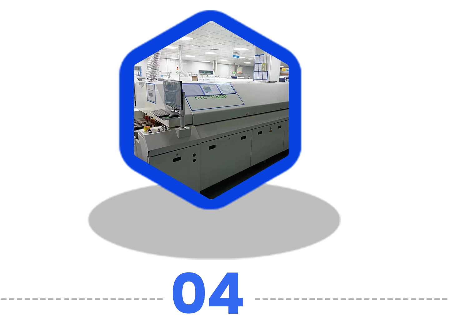 Reflow SolderingProcess Description Melt solder paste under controlled thermal profiles to form strong joints without damaging heat-sensitive components. Key Technical Requirements Multi-zone temperature profiling; peak temp control; nitrogen atmosphere (optional); thermal soak/cooling control. |
 Through-Hole Assembly (THT)Process Description Insert leaded components manually or via automation, followed by wave or selective soldering for reliable joints. Key Technical Requirements Proper lead forming; wave height control; selective solder parameters; solder fillet & hole-fill requirements. | 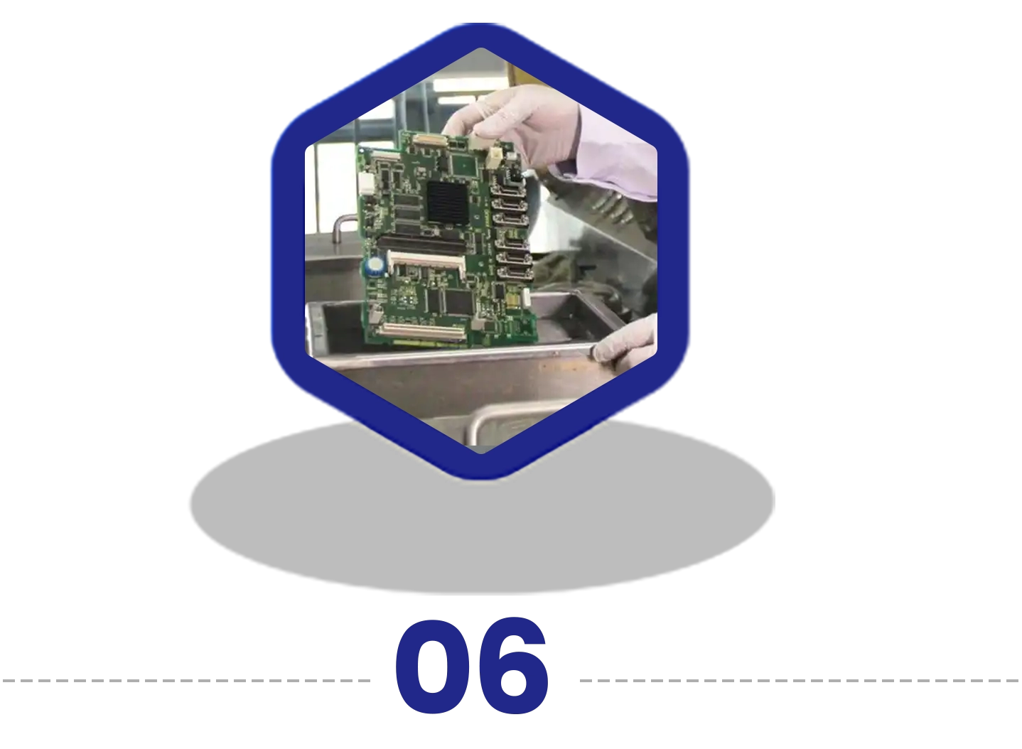 Cleaning & FinishingProcess Description Remove flux residues and apply optional conformal coating for added protection and long-term reliability. Key Technical Requirements Ionic contamination limits; ultrasonic/aqueous cleaning; controlled coating thickness; masking critical zones. | 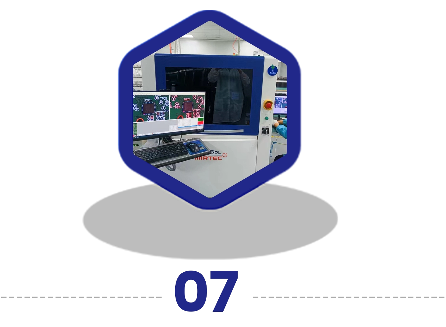 Inspection & TestingProcess Description Verify assembly quality with AOI/X-ray and confirm electrical performance through ICT, flying-probe or functional tests. Key Technical Requirements AOI coverage; X-ray for BGAs; solder joint criteria; | Discuss Your Process Requirements with Our Team |
Turnkey Supply Chain ManagementWe provide complete material procurement through authorized component distributors, lifecycle checks, counterfeit avoidance processes, and IC traceability. Consigned or hybrid sourcing models are also supported. | 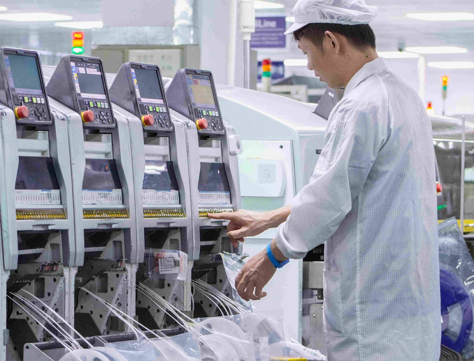 |
 | PCB Board Quality & CertificationsOur PCB board manufacturing workflow adheres to industry standards including: ISO 9001 quality management IPC-A-610 Class 2 / Class 3 workmanship RoHS / REACH compliance ESD-controlled production environment |
Applications & Industries ServedReliable PCB assembly for: Industrial control systems IoT & consumer electronics Medical devices Automotive and EV systems Communications & networking Aerospace and defense subsystems | 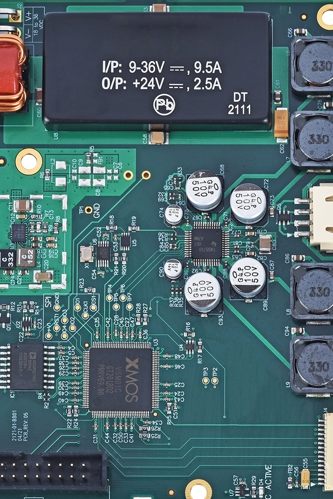 | 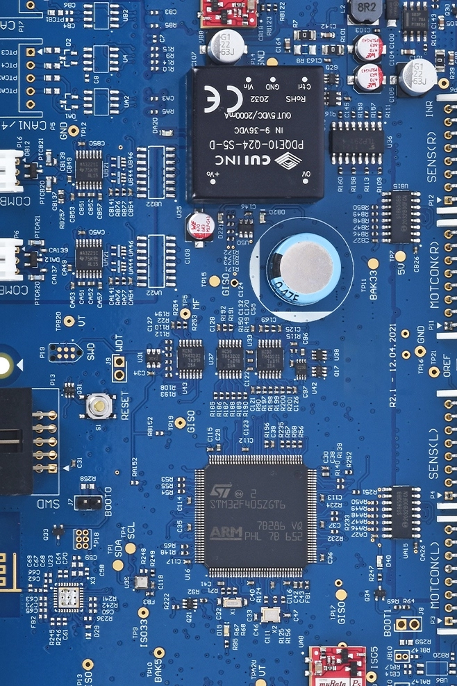 | 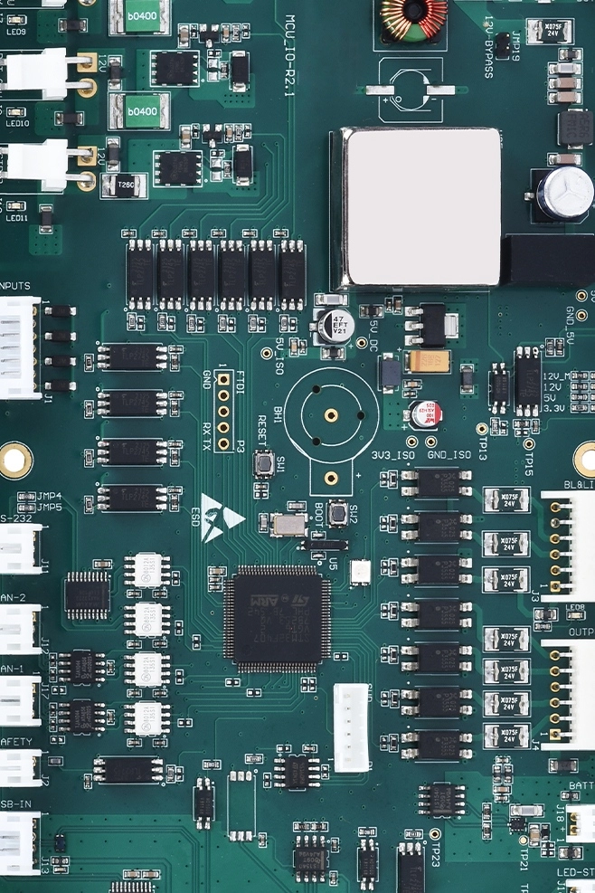 |
Proven by 7 industries, 4000+ customer projects
Please contact us at sales@knownpcb.com, ask for engineering support here or use the form below to reach out to KnownPCB | Get In Touch Today |


