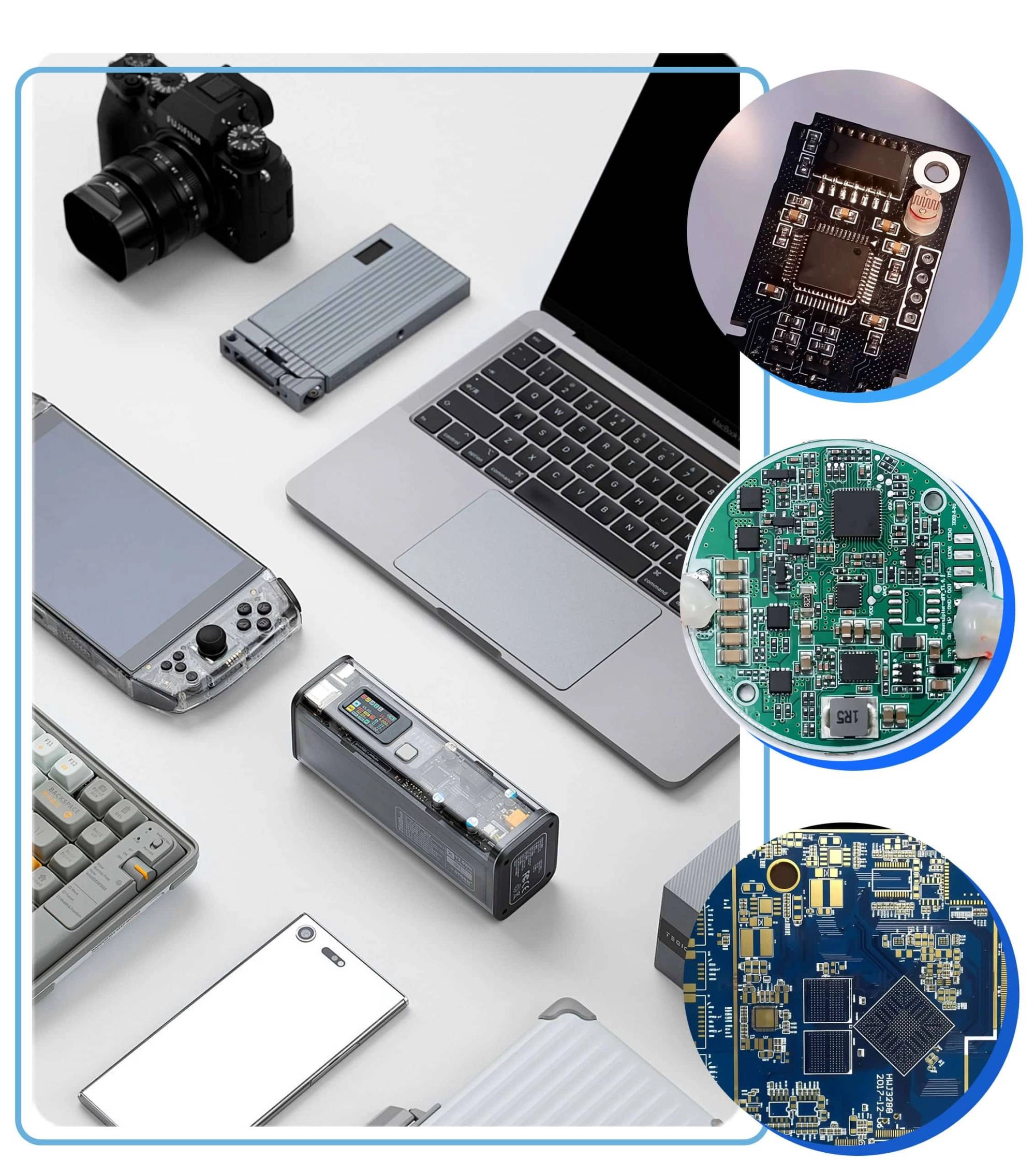
Quick Turn PCB Maker for IoT & Consumer Electronics
IoT & Consumer Electronics Push PCB Design Into Extreme Constraints. These aren't generic PCB challenges. They're problems unique to loT sized, RF-heavy , ultra-compact devices.
|  | ||||||||
Emerging constraints shaping next-generation IoT hardware design
These IoT product categories introduce different combinations of RF, mechanical, thermal, and HDI challenges.
Learn How We Solve Your Design Challenges
Application Scenario | Design Challenges | Required PCB Capabilities for IoT & Consumer Electronics |
AR/VR Headsets | - High-speed MIPI/CSI camera clusters | - Rigid-flex around optical blocks |
| - Optical/sensor sync EMI | - HDI microvia stacks for dense fan-out | |
| - Curved + compact 3D housings | - Controlled impedance for >6 Gbps links | |
| - Local compute hotspots (AI-assisted processing) | - Thermal spreading & balanced copper | |
- UWB/BLE/Wi-Fi6E coexistence
| ||
Smart Wearables | - Ultra-compact curved enclosures | - High-cycle FPC for daily motion |
| - Continuous bending & sweat exposure | - Thin-core stackups for curved geometries | |
| - Multi-radio: BLE + UWB + NFC | - RF-stable materials (low Dk/Df) | |
| - Low-power + high sensor density | - Wearable-grade rigid-flex transitions | |
- Skin-contact detuning impacting antennas
| ||
Mini IoT Modules (AIoT Nodes) | - Extremely small footprints (<15–20 mm) | - Low-loss laminates for RF sensitivity |
| - Multi-radio coexistence (BLE/Wi-Fi/UWB/LoRa) | - Controlled impedance in ultra-short RF paths | |
| - High EMC/thermal density | - HDI multilayers for dense MCU clusters | |
| - Edge AI (TinyML) causing local hotspots | - Thermal-via networks for hotspot relief | |
- Fine-pitch MCU + sensor clustering
|
These IoT product categories introduce different combinations of RF, mechanical, HDI, and thermal constraints.
 |
|
Request a Free Design Consultation
The exact engineering checks we perform for each
|
|
|
|---|---|---|
| RF interference & detuning in tight Wi-Fi/BLE/LoRa layouts | Reviewing RF keep-outs, ground returns, and coupling paths | Prevents re-tuning, sensitivity loss, and wireless failures during EVT |
| HDI fan-out congestion in multi-sensor clusters | Analyzing HDI density limits & manufacturability windows | Avoids dead-end fan-out situations and layout rework |
| Thin-core instability during reflow | Validating stackup stability, core thickness, copper balance | Prevents warpage that breaks alignment or microvia reliability |
| Thermal density inside ultra-small enclosures | Assessing copper distribution, plane design, heat paths | Reduces hotspots that only appear in real hardware |
| EMI coupling between radios and power stages | Calling out EMI/EMC risks, noisy return paths, switching edges | Prevents RF/power interference that degrades performance |
| Flex-tail failures from poor via/trace placement | Stress-checking rigid-flex transitions, bend radii, via spacing | Improves mechanical reliability in wearables & motion devices |
| Impedance shifts on crowded high-speed paths | Reviewing impedance targets, layer assignment, routing density | Prevents SI issues that appear late in EVT/DVT |
|
|
 |  |
Proven by 7 industries, 4000+ customer projects
Please contact us at sales@knownpcb.com, ask for engineering support here or use the form below to reach out to KnownPCB | Get In Touch Today |


 WHAT WE SOLVE
 WHAT WE CHECK
 WHY IT MATTERS
 Improved accuracy of optical sensors (PPG / SpO₂) through routing cleanup
 Stabilized isolation barriers in patient-contact designs
 Reduced EMI coupling between RF modules and biosignal inputs
 Increased flex-life reliability in wearable medical devices
 Prevented thermal drift in high-precision diagnostic circuits
 Improved signal consistency in multi-channel ultrasound boards
