Telecom PCB Manufacturing: Rogers® vs. FR-4 Materials
Telecom, 5G, and high-speed computing push PCBs toward ultra-low loss, tightly controlled impedance, and repeatable signal-integrity performance.
| 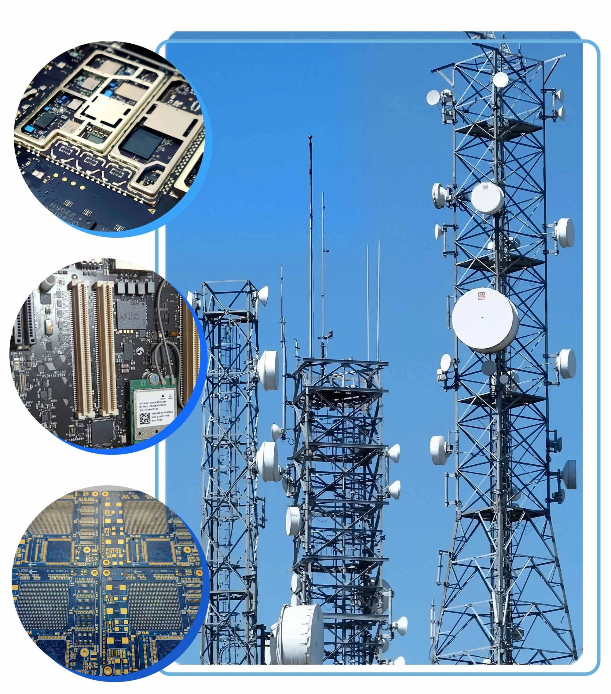 | ||||||||
Different high-speed applications introduce different combinations of frequency, loss budget, impedance, reference-plane integrity, EMI containment, and thermal behavior.
Application Scenarios & PCB Constraints
Learn How We Solve Your Design Challenges
Application Scenario | Design Challenges / Functional Needs | Required PCB Capabilities (Industry-Specific) |
5G Base Stations (Sub-6 GHz / mmWave) |
- Low-loss RF routing at multi-GHz frequencies | - Low-Dk/Df materials (Rogers, PTFE, hydrocarbon blends) |
| - Tight impedance control | - RF-optimized stackups | |
| - Isolation between RF front-end blocks | - Tight impedance (±5%) | |
- Thermal density in PA regions
| - Thermal-via grids under PA devices | |
High-Speed Networking (25G / 56G / 112G PAM4) |
- Long-reach SerDes routing | - HDI/any-layer routing |
| - Skew control between differential pairs | - Backdrilling for via-stub removal | |
| - Crosstalk and via-stub resonance | - Ultra-low-loss materials | |
- Stable reference planes
| - Tight pair matching & skew control | |
Cloud Computing / Server Boards |
- Multi-rail power integrity | - PI-optimized copper distribution |
| - High-speed lanes across long boards | - Controlled-impedance high-speed layers | |
| - Dense connectors & backplane transitions | - Reinforced planar structures | |
- Thermal management in CPU/ASIC zones
| - Hybrid stackups (RF + digital + power) | |
Edge-Computing / Networking Appliances |
- Compact form factor with high bandwidth | - Low-loss multilayers |
- EMI containment
| - RF-shielding stackup strategies |
High-speed stackups depend heavily on materials and geometry.
These are not “capabilities”—they are constraints imposed by 5G, SerDes, and high-bandwidth systems.
 |
|
Request a Free Design Consultation
The exact signal-integrity (SI) and power-integrity (PI) checks we perform for telecom, networking, and high-speed computing platforms include:
|
|
|
|---|---|---|
| Loss too high on long-reach SerDes lanes | Loss budget per inch, material selection, via transitions | Ensures sufficient eye-margin at 25G / 56G / 112G |
| Impedance drift in dense routing | Stackup tolerance, dielectric variation, copper roughness | Avoids reflections and jitter accumulation |
| Crosstalk between differential pairs | Pair spacing, layer assignment, plane discontinuities | Keeps signal integrity under dense routing |
| Via-stub resonance | Backdrill depth, stub length, via type | Prevents resonance at SerDes Nyquist frequencies |
| RF front-end detuning | Ground returns, RF keep-outs, cavity effects | Keeps PA / LNA behavior predictable |
| PI instability under high load | Copper distribution, decoupling strategy, return paths | Stabilizes CPU / ASIC performance |
| Transition losses through connectors / backplanes | Launch geometry, anti-pad optimization | Minimizes insertion and return-loss penalties |
|
|
 |  |
Proven by 7 industries, 4000+ customer projects
Please contact us at sales@knownpcb.com, ask for engineering support here or use the form below to reach out to KnownPCB | Get In Touch Today |


 WHAT WE SOLVE
 WHAT WE CHECK
 WHY IT MATTERS
 Eliminated via-stub resonance through backdrilling
 Improved RF front-end impedance stability for 5G PA/LNA modules
 Stabilized PI for high-current CPU / ASIC boards
 Reduced crosstalk across dense high-speed layers
 Optimized launch geometry for backplane connectors
 Maintained impedance tolerance across hybrid RF / digital stackups
