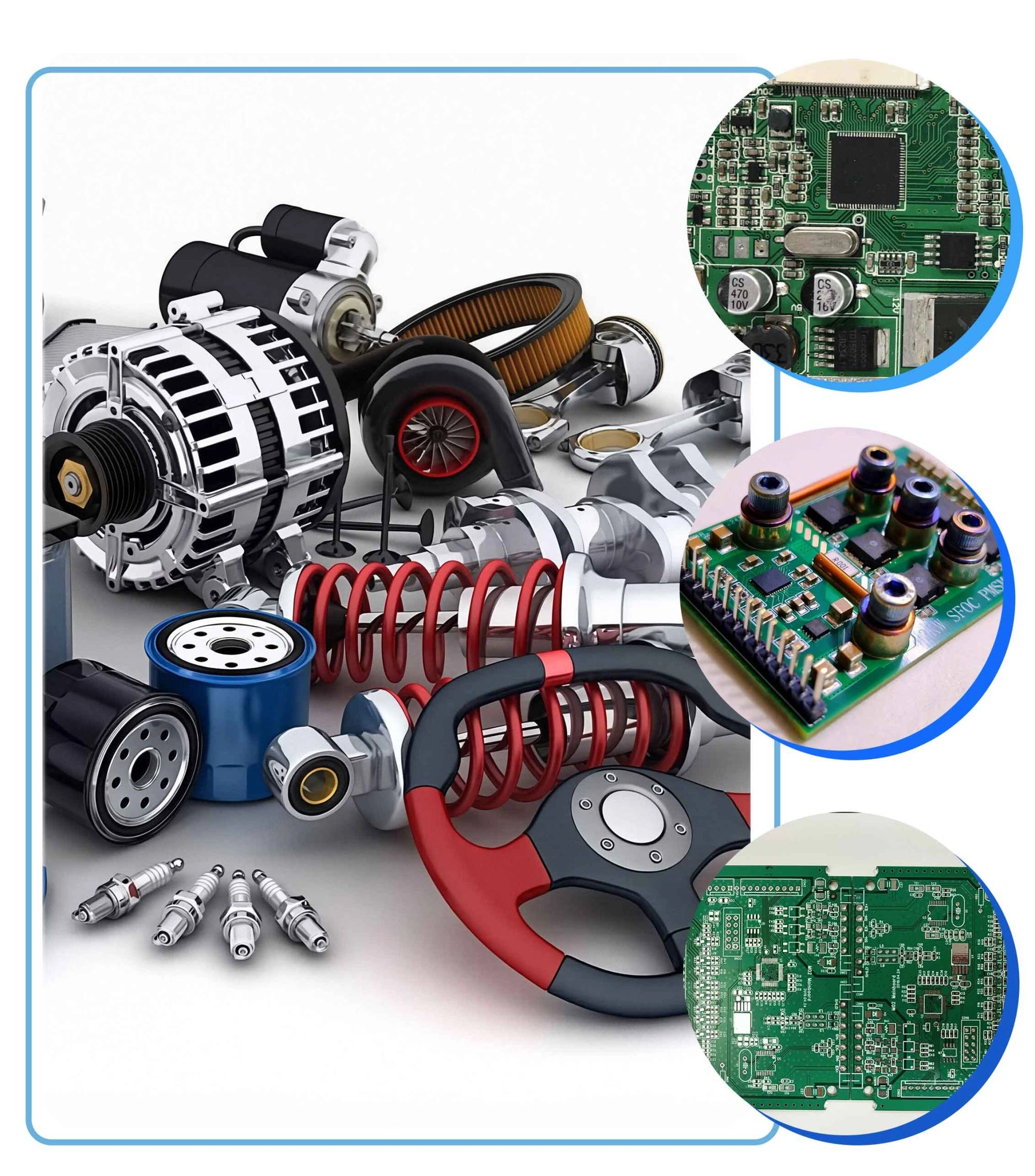
Automotive PCB Supplier with PPAP Documentation Support | |||||
| 01 EV platforms introduce additional complexity—fast-switching SiC inverters, high-current HV buses, dense BMS monitoring, and mixed-signal electronics that must survive a decade (or more) of thermal cycling. | |
| 02 Automotive electronics operate under conditions that normal consumer hardware will never experience —heat, cold, vibration, high voltage, electrical transients, long duty cycles, and strict safety expectations. |
Design for High Voltage, Vibration, Thermal Cycling, and Safety Compliance
Learn How We Solve Your Design Challenges
Application Scenario | Design Challenges / Functional Needs | Required PCB Capabilities (Industry-Specific) |
EV Battery Management Systems (BMS) |
- HV isolation between sensing & power | - High-isolation stackups |
| -Accurate sensing over long wiring harnesses | - HV creepage/clearance spacing | |
| - High-voltage transients | - Low-drift sensing routing | |
- Mixed digital/analog stability
| - High-CTI materials for EV environments | |
Inverter / Motor-Control Units |
- Fast-switching SiC / IGBT thermal density | - Heavy-copper planes |
| - High-current loops | - Low-inductance power paths | |
| - EMI/EMC from switching edges | - EMI-aware isolation layout | |
- Vibration & thermal cycling stress
| - Reinforced mechanical reliability | |
On-Board Chargers (OBC) / DC-DC Converters |
- Wide temperature range (–40°C to 125°C) | - Thermal-via grids |
| - High voltage & HF switching | - Thick dielectric for HV layers | |
| - Isolated power stages | - HV isolation stackups | |
- Thermal hotspots in compact enclosures
| - Materials stable under HF switching | |
ADAS / Camera / Radar Modules |
- High-speed SerDes (MIPI/FPD-Link) | - Controlled-impedance HDI |
| - Sensor fusion EMI | - Low-loss materials | |
| - Cold-start condensation | - Shielded stackup strategies | |
- Long-distance harness noise
| - Moisture-resistant laminates | |
Automotive Lighting / Body Control |
- High-temperature ambient exposure | - High-Tg materials |
| - Large current distribution | - Copper balancing for thermal cycling | |
- Long lifetime expectations
| - Robust plating & via integrity |
These are not capabilities—they are industry-imposed constraints required for safe, long-life automotive electronics.
 | Automotive stackups are defined by:
|
Request a Free Design Consultation
The exact engineering checks we perform for each project include:
|
|
|
|---|---|---|
ISO 7637-2 transient & load-dump vulnerability | Reviewing input protection (TVS), filtering, grounding, and return paths | Prevents resets, latent damage, and field failures during vehicle transients |
HV isolation gaps and routing in compact layouts | Validating creepage/clearance, slots/keepouts, coating strategy, CTI/material limits | Reduces arcing risk and supports functional safety and HV compliance |
Partial discharge risk in HV nodes and edges | Flagging sharp copper edges, void-prone structures, spacing at HV transitions | Avoids insulation degradation that shows up after thermal cycling |
Thermal hotspots in high-current paths (inverters, DC-DC, busbars) | Assessing copper weight, current density, via stitching, heat spreading and sinking paths | Prevents overheating, delamination, and accelerated aging |
EMI coupling from power stages into sensing/communication | Calling out noisy return paths, switching loops, partitioning, and shielding opportunities | Improves CISPR 25 margin and reduces intermittent performance issues |
Vibration-driven fatigue at connectors and heavy components | Stress-checking anchor points, pad/trace reinforcement, teardrops, stiffeners, and stackup rigidity | Reduces cracked joints and intermittent opens under vibration profiles |
Corrosion susceptibility in harsh environments (salt fog, moisture) | Reviewing surface finish, edge plating needs, conformal coating coverage, and leakage paths | Prevents leakage, dendrites, and long-term reliability drift |
SI integrity on automotive high-speed links (CAN FD / Ethernet) | Reviewing impedance targets, pair routing, reference continuity, skew, and stubs | Avoids late-stage link instability and EMI surprises |
|
|
 |  |
Proven by 7 industries, 4000+ customer projects
Please contact us at sales@knownpcb.com, ask for engineering support here or use the form below to reach out to KnownPCB | Get In Touch Today |


 WHAT WE SOLVE
 WHAT WE CHECK
 WHY IT MATTERS
 Stabilized SiC inverter loops to reduce EMI hotspots
 Improved BMS sensing accuracy under long harness lengths
 Reduced HV creepage failures in EV battery stages
 Reinforced via structures for high-vibration zones
 Improved ADAS SerDes signal integrity in low-loss stackups
