We strategically place low Df laminates on critical layers and combine them with
economical high-Tg cores, drastically lowering the BOM cost for your low-to-mid volume run.

Consult our Application Engineers (AEs) today to design an optimized stack-up that balances Dk stability and budget for your 5G small cell prototype.
High frequency PCB optimized for RF, microwave and mmWave circuits where low loss and stable impedance are critical.
Qualification Materials & Compliance OverviewAcceptance StandardsQualified to IPC-6012 / IPC-6018 (where applicable) with RF-specific tests for impedance and loss. High Frequency PCB Material StandardsPTFE, hydrocarbon-ceramic or other low-Dk / low-Df laminates, sometimes in hybrid stacks with FR-4; material grades traceable. StructureControlled-impedance stack-up with RF layers, carefully designed reference planes and via structures to minimise discontinuities. ComplianceSupports RoHS / REACH, UL where required, and telecom/industrial standards for temperature, humidity and reliability. |
KnownPCB Prototyping & Mass Production Service Ask for DFM Guideline
Premium material and process, justified when RF performance drives product value.
| 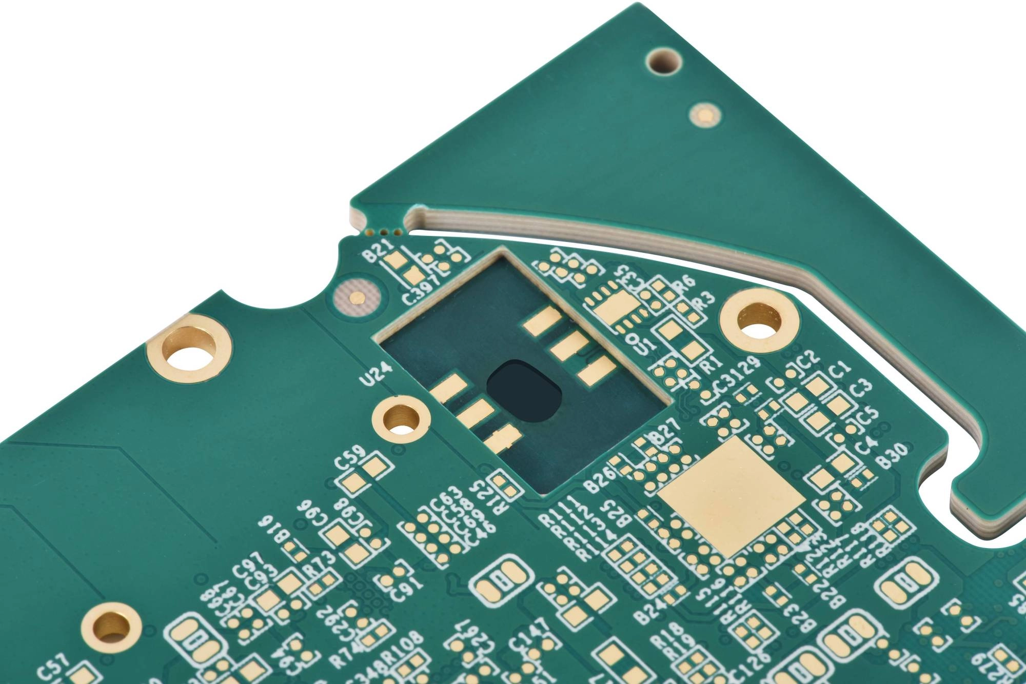 |
 | Optimized for RF, microwave and mmWave signal integrity.
|
KnownPCB Prototyping & Mass Production Service Ask for DFM Guideline
High-Frequency PCB fabrication demands extreme precision. We utilize LDI for fine-line definition and Plasma Desmear for clean via barrels. Critical steps include specialized RF Material Cutting to manage Dk stability, finalized by rigorous TDR Testing to verify impedance control and signal integrity. KnownPCB Profile Ask for DFM Guideline | 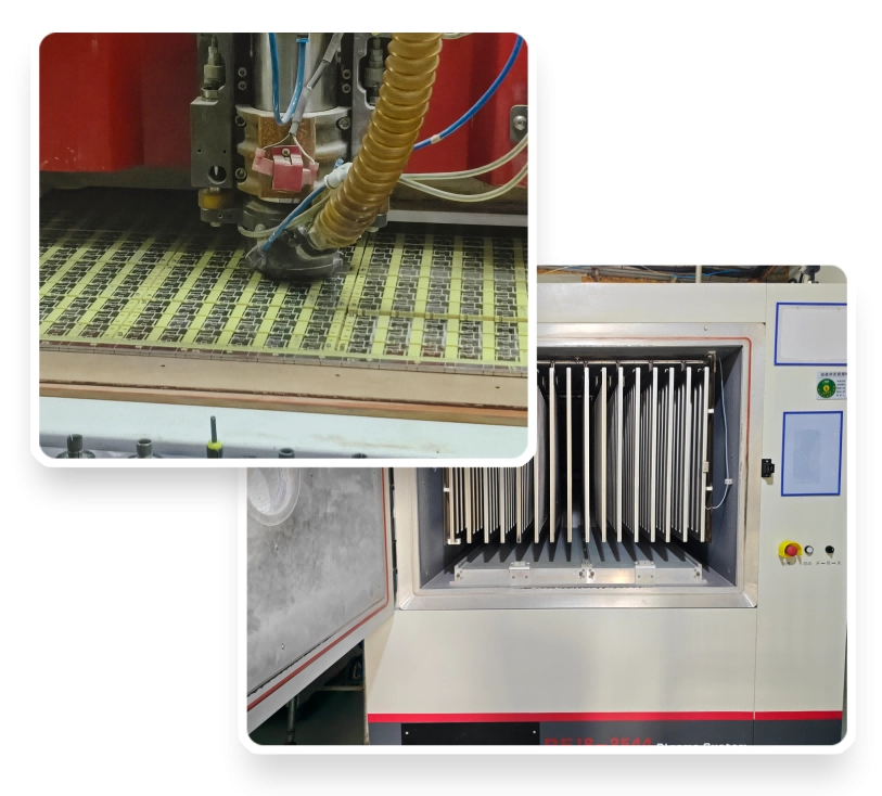 |
| Category | Parameter | Dissipation Factor (Df @10 GHz) | Frequency Range | Tg (°C) | TCDk (ppm/°C) | Thermal Conductivity (W/m·K) | Standard Thickness (mm) | Typical Applications |
| RF / Microwave | General low-loss laminates | 0.0037 | Up to ~10 GHz (RF / Microwave) | >280 | ~50 | 0.62 | 0.10–3.20 | 5G antennas, RF front-end modules, radar |
| RF Circuits | Low-loss RF circuits | 0.0027 | 1–8 GHz RF circuits | >280 | ~40 | 0.71 | 0.10–2.00 | IoT wireless modules, WLAN, L-band microwave |
| mmWave | Ultra-low loss for 77 GHz class | 0.0013 | Up to 77 GHz (mmWave) | >280 | ~13 | 0.5 | 0.13–2.00 | Automotive 77 GHz radar, 5G mmWave phased arrays |
| High-Dk | Microwave miniaturization | 0.0027 | High-Dk microwave miniaturization | >280 | Typical | Varies | Varies | Compact microwave antennas & filters |
| RF / Microwave | Wideband RF materials | 0.0022 | 1–30 GHz RF / Microwave | >280 | ~23 | 0.64 | 0.25–2.00 | High-Dk couplers, resonators, amplifiers |
| High-Reliability | High-reliability RF laminates | 0.0037 | Up to ~10 GHz (High-reliability) | >280 | ~50 | 0.69 | 0.10–3.20 | Aerospace & high-reliability RF modules |
| PTFE-based | Cost-effective broadband RF | 0.0018–0.0030 | 1–40 GHz RF & microwave | ~280 (PTFE-based) | ~50 | 0.25 | 0.13–3.20 | Cost-effective RF boards, antennas, broadband circuits |
| mmWave | Very low loss for 110 GHz class | 0.0009 | Up to 110 GHz (mmWave) | >280 | <50 | ~0.20 | 0.127–3.175 | mmWave radar, satellite communication, broadband RF |
| High-Dk | High-Dk microwave circuits | 0.0027 | Up to ~40 GHz | >280 | ~50 | ~0.24 | Varies | High-Dk microwave circuits |
| Ultra-compact RF | Filters & resonators | 0.0023 | 1–40 GHz | >280 | ~50 | ~0.24 | Varies | Ultra-compact RF filters & resonators |
| Thermal Optimized | High-power RF / microwave | Low (thermal optimized) | High-power RF / microwave | >280 | — | Enhanced thermal conductivity | Varies | RF power amplifiers, phased-array transmit modules |
| Thermal Substrates | High-frequency + high power | 0.0003–0.0005 | High-frequency + high power | — | Very stable | 20–30 | 0.25–2.0 | High-power microwave modules, LED thermal substrates |
| High-Heat Load | High-frequency + high heat load | ~0.0003 | High-frequency + high heat load | — | Very stable | 150–200 | 0.25–2.0 | Radar TR modules, satellite payloads, mmWave PA |
Get a FREE DFM Review on Your Design (24-Hour Feedback)
| Category | Parameter | STANDARD (Sub-6G / ISM / WiFi / Entry RF) | ADVANCED (Microwave 6–18 GHz / Mid-band 5G) | MICRO (mmWave 18–40+ GHz / Radar / Antenna Array) | Classification Logic | Typical Use Case |
| RF Band | Target Frequency Band | <6 GHz (Sub-6G, ISM, WiFi 2.4/5G) | 6–18 GHz (C/X/Ku, Mid-band 5G, Microwave Links) | 18–40+ GHz (Ka, mmWave, Radar, Phased Array) | RF Band / Application | Quick band-based selection for engineers & buyers |
| System Use | Application Scenario | Wireless modules, routers, small cells, high-speed mixed-signal | 5G AAU, microwave front-end, radar front-end | mmWave radar, Ka-band terminals, precision phased arrays | Band / System Use | Sales & procurement tier by end-application |
| Stack-up | Layer Count | 2–6 layers, simple mixed-signal | 4–10 layers, high-speed + RF hybrid | 8–16+ layers, complex RF + digital + power isolation | Stack-up Complexity | Engineer stack-up & cost assessment |
| Stack-up / Layout | Typical RF Structure | Single/dual microstrip + simple planes | Multi-plane w/ Microstrip + Stripline mix | Multi-plane w/ multi-stripline + shielding layers | Stack-up / Layout | RF designer’s stack-up planning |
| Material Options | Base Material | High-Tg FR-4 / Low-loss FR-4 / Mixed laminate | Rogers 4000 / Isola I-Tera / Panasonic Megtron (hybrid stack-ups) | PTFE / LCP / Advanced RF materials (Rogers 3000/6000 series) | Material / Process | RF material selection for SI & loss |
| Material | Typical Dk (10 GHz) | ~3.5–4.2 | ~3.0–3.7 | ~2.2–3.0 | Material / Process | Impedance & phase design |
| Material | Df @ 10 GHz | ~0.008–0.015 | ~0.003–0.008 | ≤0.003 | Material / Process | HF/microwave loss budgeting |
| Material | Copper Type | Standard ED (standard roughness) | Low-roughness ED / Half-gloss copper | Ultra-low-roughness ED / RA / VLP copper | Material / Process | Control insertion loss & reflection |
| Surface Finish | — | HASL / OSP / ENIG | ENIG / ENEPIG | ENIG / ENEPIG / Selective soft-gold for RF ports | Material / Process | RF connectors / SMA pad reliability |
| Impedance Control | Impedance Tolerance | ±10% | ±7–10% | ±5% or tighter | Functional / SI | RF-SI design requirements |
| Insertion Loss | Insertion Loss Target (relative) | Baseline IL control | Optimized IL for 6–18 GHz | Ultra-low IL for mmWave / long RF chains | Functional / SI | Link budget / range / sensitivity |
| Electrical Testing | Test Method | Flying probe + partial TDR | TDR + S-parameter checks on critical links | Full S-parameter validation (VNA) + 100% key-link sampling | Functional / Quality | Buyer verification of electrical reliability |
| Via Structure | Via Structure | Through-hole dominant, limited backdrill | Through-hole + blind/buried vias; routine backdrill for key SerDes | TH + blind/buried + Via-in-Pad; system-level backdrill | Layer / Structure | Minimize via stubs & improve return loss |
| Process | Via-in-Pad | Optional in BGA areas | Recommended for dense BGA & high-speed links | Mandatory for mmWave ICs, RF BGAs, front-end chips | Process / Layout | Packaging & placement capability indicator |
| SI Optimization | Backdrilling Usage | Limited high-speed interfaces | Routine on differential SerDes links | Extensive multi-stage backdrilling | Functional / SI | Improve eye diagram & reduce stub resonance |
| Routing | Min. Trace / Space | 0.10 mm (4 mil) | 0.075 mm (3 mil) | 0.05 mm (2 mil) or below | Material / Process | High-density RF routing |
| Stack-up | Board Thickness | 0.6–1.6 mm | 0.6–2.0 mm | 0.8–2.4 mm (multi-plane / shielding capable) | Stack-up | Impedance, connector fit, mechanics |
| Dielectric Control | Dielectric Thickness Control | Standard FR-4 tolerance | Optimized dielectric thickness (impedance-oriented) | Precision dielectric thickness (phase / delay critical) | Material / Process | Phase match & differential delay |
| Reliability | Operating Temperature | 0–85 °C | –20 to 105 °C | –40 to 125 °C or above | Functional / Reliability | Telecom / automotive / industrial |
| Reliability Standard | Reliability Class | IPC-6012 Class 2 | IPC-6012 Class 2/3 | IPC-6012 Class 3 / telecom & automotive grade | Functional / Quality | Buyer/engineer quality alignment |
| Tier | Service Tier | High-Frequency PCB STANDARD | High-Frequency PCB ADVANCED | High-Frequency PCB MICRO/mmWave | Tier / Capability | Procurement tier by project value |
| Schedule | Standard Lead Time | 7–10 days | 10–15 days | 8–18+ days (freq/material dependent) | Schedule | RF prototype / pilot planning |
| RF Layout | RF Structure Optimization | Basic RF widths/spacings + simple impedance ctrl | Added reference grounds, impedance via arrays, simple coupling structures | Full RF layout rules: via fences, moat grounds, phase matching | Functional / SI | RF layout & SI co-design |
| EMC / Isolation | Shielding & Isolation | Copper pour + simple ground split | Local shielding areas + stitched grounds | Multi-zone shielding + metal-can interface provisions | Functional / EMC/EMI | Reduce crosstalk, improve RF/EMC |
Get a FREE DFM Review on Your Design (24-Hour Feedback)
Industry-specificPCB SolutionsLearn about KnownPCB & Production equipments |
What questions matter most in high-frequency and high-speed PCB design?
From controlled impedance stackup, low-loss laminate selection, and DDR/PCIe routing rules to mass-production tolerances, testing methods, and storage conditions, these FAQs help engineers optimize cost, lead time, and signal integrity with factory-level guidance.
For deeper technical discussions, feel free to reach out to KnownPCB.
Proven by 7 industries, 4000+ customer projects
Please contact us at sales@knownpcb.com, ask for engineering support here or use the form below to reach out to KnownPCB | Get In Touch Today |