Engineered for High-Current and High-Thermal Performance.
Our specialized etching process guarantees excellent Etch Uniformity and Wall Plating Adhesion,
critical for embedded high-current Busbars and integrated heat sink solutions in demanding power systems.

PCB with significantly increased copper thickness for high current and high thermal load applications.
Qualification, Materials & Compliance OverviewAcceptance StandardsTested to IPC-6012 with additional coupons for heavy copper plating thickness and adhesion. Material StandardsHigh-Tg FR-4 or enhanced thermal FR-4, copper weights typically ≥ 3 oz on selected layers, UL-listed constructions. StructureReinforced copper planes and wide traces, often with multiple ounce copper in internal or outer layers for power paths. ComplianceDesigned to meet RoHS / REACH, UL, and IEC/UL safety distances for power electronics and high-voltage sections. |
KnownPCB Prototyping & Mass Production Service Evaluate Your High-Current PCB Design
(Heavy Copper Printed Circuit Board)
Higher material and processing cost, offset by simpler power hardware.
|  |
 | Focused on power handling and thermal behaviour rather than extreme density.
|
KnownPCB Prototyping & Mass Production Service Evaluate Your High-Current PCB Design
Heavy copper PCB production is highly specialized. We rely on the Thick Copper Plating Line to guarantee uniform oz distribution throughout the barrel and surface. High current designs demand more than thicker copper. The table below clarifies practical limits for copper weight, trace spacing, plating cycles, and thermal performance—helping you determine when heavy copper is justified, and how power density, reliability, and cost scale with copper thickness. KnownPCB Profile Ask for DFM Guideline | 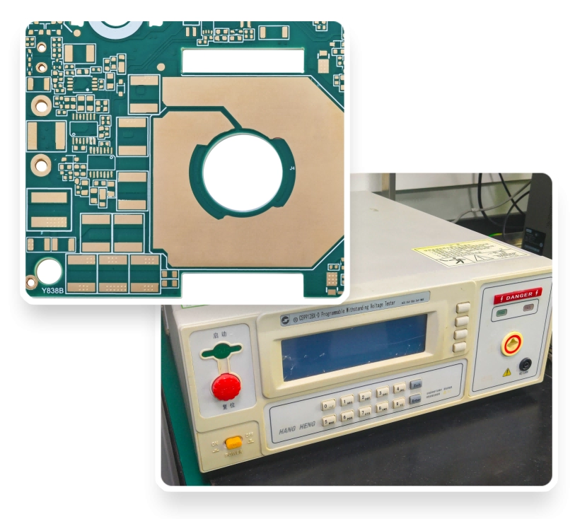 |
| Parameter | BASIC (2–3 oz) | ADVANCED (4–6 oz) | HIGH-END (8–10 oz +) | Notes / Engineering Reference | Classification Logic |
| Layer Count | 2–4 Layers | 4–8 Layers | 8+ Layers, incl. local heavy-copper zones | Identifying power-stage / high-current sections | Layer Count / Stack-up |
| Copper Weight | ≤20 oz | ≤20 oz | ≤20 oz | High-current / high-power-density applications | Material / Process |
| Base Material | Standard FR-4 (130–140 Tg) | High-Tg FR-4 (170–180 Tg) | High-Tg FR-4 / High-performance resin system | High-temperature & high-current environments | Material / Process |
| Surface Finish | HASL / OSP | ENIG / OSP | ENIG / Hard Gold / Selective plating | Terminals, power connectors, high-wear pads | Material / Process |
| Current-carrying Capability (Typical Ampacity) | 10–20 A / trace (width-dependent) | 20–40 A / trace | 40 A+ / bus-bar-like structures | Used for power design & trace-width selection | Functional / Performance |
| Voltage Drop & Temperature Rise | Moderate control | Optimized voltage drop & ΔT | Strict ΔV/ΔT control + hotspot suppression | Reliability vs. efficiency | Functional / Performance |
| Minimum Trace / Space | ≥0.15 mm | ≥0.25 mm (due to thick copper) | ≥0.30 mm (extreme copper) | Manufacturability review / IPC constraints | Material / Process |
| Drilling & Copper Plating | Standard plated through-holes | Thick copper plating | Ultra-thick copper / multi-step plating cycles | Via ampacity / reliability | Material / Process |
| Thermal Cycling Life | Standard grade | Enhanced grade (Power / Industrial) | Automotive / Special-certification grade | Long-term load endurance | Functional / Performance |
| Max Operating Temperature | ~170 °C | ~170 °C | ~180 °C+ | High-temp & thermal-design requirement | Functional / Performance |
| Service Tier | Heavy Copper | Heavy Copper ADV | Heavy Copper PRO | Procurement differentiation by power class | Service Tier / Capability |
| Typical Lead Time | 5–15 days | 5–20 days | 7–25 days | Project planning & supply lead time | Schedule / Planning |
| Local Heavy-Copper Region | Full-board uniform copper | Partial high-current zone enhancement | Complex multi-region heavy-copper / multilayer copper stacking | Power-stage zoning / control-path separation | Material / Process |
| Thermal Design | Basic copper pour for heat spreading | Copper pour + thermal vias | Heavy-copper + thermal vias + heat-spreader blocks (integrated) | High-power module thermal architecture | Functional / Performance |
Industry-specificPCB SolutionsLearn about KnownPCB & Production equipments |
Copper thickness, current capacity, and thermal paths define heavy copper PCB reliability.
These FAQs explain stackup planning, etching control, plating uniformity, and qualification testing, supporting stable high-power PCB manufacturing with predictable cost and delivery.
Request Heavy Copper Design Review
Proven by 7 industries, 4000+ customer projects
Please contact us at sales@knownpcb.com, ask for engineering support here or use the form below to reach out to KnownPCB | Get In Touch Today |