We specialize in highly complex Multilayer Boards (MLBs).

We use high TG, laminates to guarantee dimensional stability and long-term vibration resistance for industrial and defense applications.
Consult our Application Engineers (AEs)
General-purpose workhorse for control, digital and mixed-signal designs, typically 4–12 layers.
Qualification, Materials &Compliance OverviewAcceptance StandardsBuilt and inspected per IPC-6012 Class 2 / Class 3 and IPC-A-600. Material StandardsFR-4 or mid-loss FR-4 materials, with Tg/Td selected to match the product temperature profile; UL-recognized. Structure OverviewMultiple copper layers with buried and through vias, defined prepreg/core stack-up, and dedicated power/ground planes. ComplianceSupports RoHS / REACH, UL marking, and creepage/clearance rules aligned with relevant IEC/UL safety standards. |
KnownPCB Prototyping & Mass Production Service Ask for Layout Optimization Guideline
Baseline cost option for 4–12 layer designs.
|  |
 | Balanced electrical behaviour for common high-speed and mixed-signal designs.
|
KnownPCB Prototyping & Mass Production Service Ask for Layout Optimization Guideline
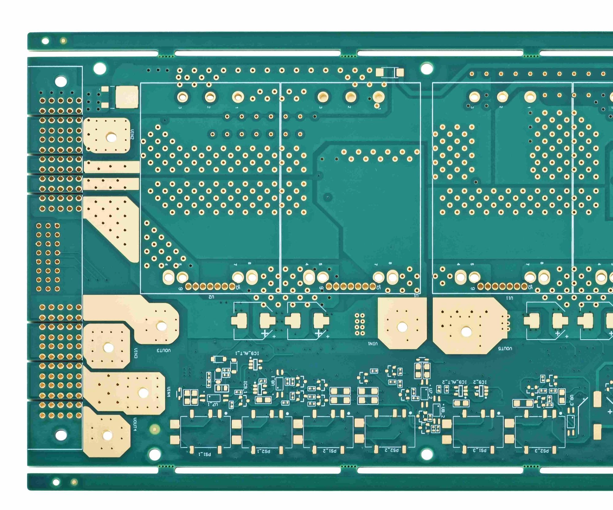
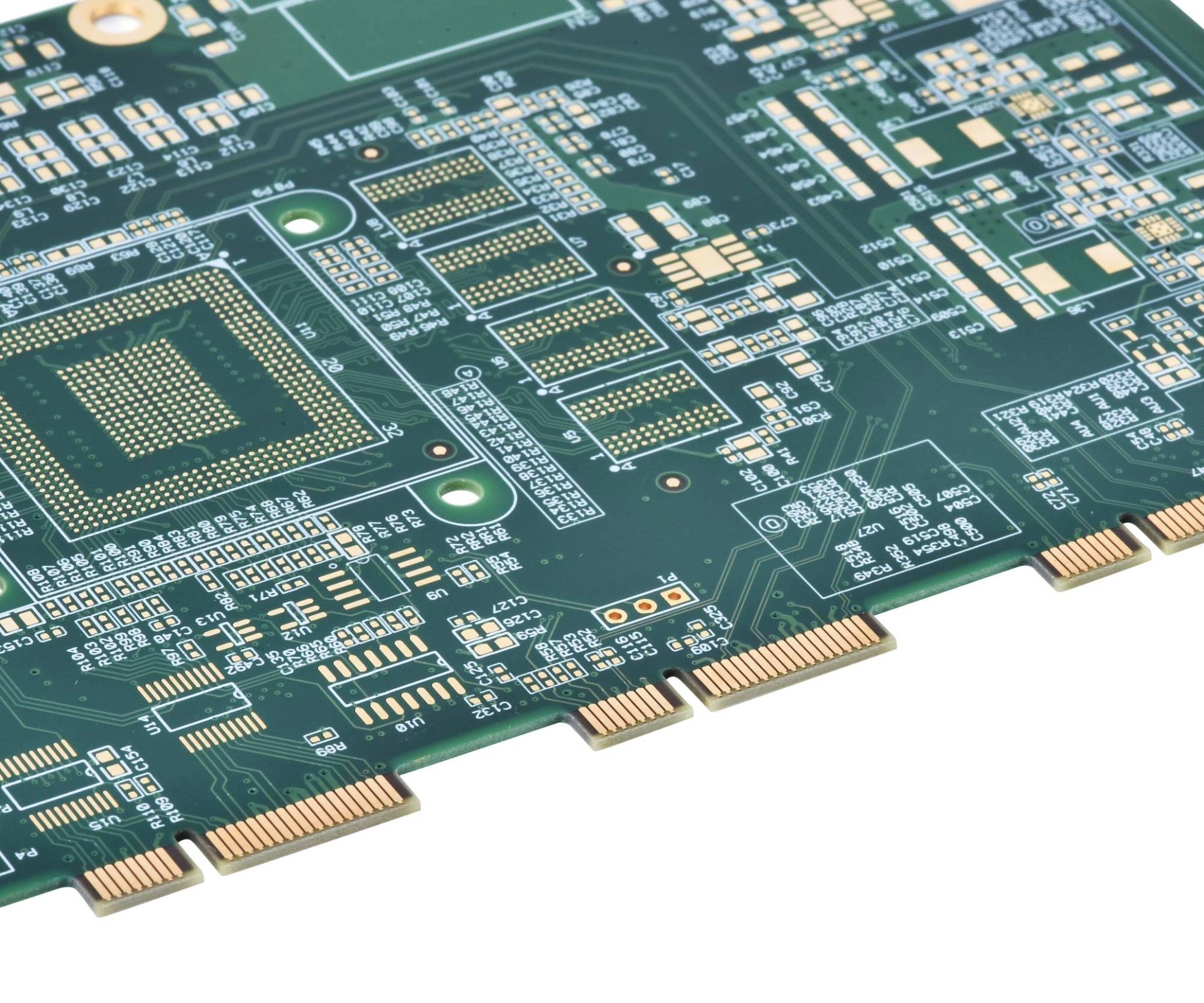
Multilayer PCB fabrication requires extreme control over structural integrity. We implement Inner Layer AOI for zero-defect verification before lamination. Core steps include Vacuum Lamination to ensure void-free layer bonding, followed by precise Through-Hole Drilling and robust Plating to guarantee reliable inter-layerconductivity and high Aspect Ratio support. This table summarizes what standard multilayer PCBs can reliably support—from 4 to 20+ layers—so you can judge cost, signal behavior, and manufacturability before committing to HDI or special processes. KnownPCB Profile Ask for DFM Guideline |  |
| Parameter | BASIC (4–6 Layers) | ADVANCED (8–12 Layers) | HIGH-END (14–24+ Layers) | Complexity Trend | Classification Logic | Typical Use Case |
| Layer Count | 4–6 Layers | 8–12 Layers | 14–24+ Layers (incl. backplane / complex system boards) | ↑ More layers → ↑ Complexity | Layer Count / Stack-up | Quick structural assessment for engineers |
| Application Positioning | General control boards | High-speed signal + control hybrid boards | Core logic boards / Backplanes / Server motherboards | ↑ System importance | Application / Architecture | Project tiering & complexity |
| Base Material | Standard FR-4 | High-Tg FR-4 / Partial low-loss laminates | High-Tg / Low-loss (e.g., Megtron/Rogers hybrid) | ↑ Performance requirements | Material / Process | Signal integrity / thermal performance |
| Typical Stack-up | 1–2 power planes + signal layers | Multiple power planes + high-speed differential layers | Multi-plane + high-speed diff pairs + shielding layers | ↑ Finer stack-up planning | Layer Structure | Designer stack-up planning |
| Surface Finish | HASL / OSP | ENIG / OSP | ENIG / ENEPIG / Selective plating | ↑ HDI-friendly finishes | Material / Process | BGA/QFN solder reliability |
| Finished Board Thickness | 0.2–1.6 mm | 0.4–2.0 mm | 1.6–3.0 mm (incl. backplane options) | ↑ Thickness & rigidity | Structure / Mechanical | Connector engagement / structural stiffness |
| Min. Trace / Space | 0.075 mm | 0.075 mm | 0.05 mm or smaller (2 mil class) | ↑ Tighter routing density | Material / Process | High-density routing |
| Mechanical Drill Size | 0.15 mm | 0.15 mm | 0.125–0.15 mm | ↓ Drill size | Stack-up / Via Design | Via / connector compatibility |
| Impedance Control | Partial critical signals | Full critical high-speed channels | Full-board impedance control incl. diff pairs & backplane channels | ↑ More impedance-controlled lines | Functional / Performance | High-speed interface planning |
| Supported Data Rates | ≤1–2 Gbps | ≤5–10 Gbps | 10–25+ Gbps (differential) | ↑ Higher rate capability | Functional / Performance | Protocol selection (PCIe / USB / SERDES) |
| Operating Temp Range | 0–85 °C | –20 to 105 °C | –40 to 125 °C | ↑ Environmental robustness | Functional / Performance | Industrial / automotive |
| Reliability Standards | IPC-6012 Class 2 | Class 2 / Class 3 | Class 3 / Special certifications | ↑ Certification level | Functional / Performance | Quality grade alignment |
| Service Tier | Multilayer BASIC | Multilayer ADV | Multilayer PRO | ↑ Engineering support required | Tier / Capability | Procurement & engineering decision |
| Standard Lead Time | 7–10 days | 10–15 days | 15–20+ days | ↑ Lead-time vs. layer count | Schedule / Planning | Project scheduling |
| Blind / Buried Vias | None or minimal | Single-direction buried vias | Multi-stage blind/buried vias + local HDI | ↑ Via structure complexity | Material / Process | Works with HDI / fine-pitch |
| Backdrilling | Optional | Standard for high-speed links | Extensive backdrilling + long-reach diff-pair optimization | ↑ SI optimization needed | Functional / Performance | Stub removal / eye-diagram optimization |
Industry-specificPCB SolutionsLearn about KnownPCB & Production equipments |
What should engineers confirm before multilayer PCB manufacturing?
These FAQs cover stackup design, layer-to-layer registration accuracy, impedance control, and production tolerances, helping optimize signal integrity, cost efficiency, and delivery reliability with factory-level manufacturing guidance.
For deeper technical discussions, feel free to reach out to KnownPCB.
Proven by 7 industries, 4000+ customer projects
Please contact us at sales@knownpcb.com, ask for engineering support here or use the form below to reach out to KnownPCB | Get In Touch Today |