 +86 755 2794 4155
  sales@knownpcb.com
-
Shenzhen KNOWNPCB Technology Co., Ltd.
 +86 755 2794 4155
  sales@knownpcb.com

Have you noticed that now more and more of our lighting is using led lighting.What is LED? Compared to the traditional light bulbs, LEDs have lower power consumption, longer lifetime and higher energy efficiency. In the PCB industry,when we say LED PCB, it refers to the pcb used for LED lighting, if you are looking for a suitable LED PCB for your lighting system, this article may bring you something. WHAT ARE LEDS COMPOSED OF?LED is an initial light-emitting diode that produces light when an electric current passes through. LEDs typically have negative and positive electrodes, which generate light in the visible light region.The LEDS are glued to the PCB by soldering process and have electrical connections for lighting.Since light-emitting diodes dissipate a lot of heat when they are in use, when you are designing LED, the metal core is usually the best choice for LED PCB, it is because that it dissipates heat more faster. Among them, the metal material aluminum is the most widely used
1. Capacitors generally use "C" and numbers in the circuit (such as a capacitor with a number 13 in C13). The capacitor is two pieces of gold Components composed of the membrane are tight and are separated by insulating materials in the middle. The characteristics of capacitors are mainly DC communication. The size of the capacitor capacity is to indicate the size of the energy storage. The obstacle of the capacitor to the communication signal is called the capacity of the capacity. The frequency of flow signal is related to electricity capacity. Rong resistance XC = 1/2πf C (f represents the frequency of the communication signal, C represents the capacitor capacity) The types of capacitors commonly used in the telephone are electrolytic capacitors, porcelain capacitors, patch capacitors, monopolic capacitors, 钽 capacitors and polyester capacitors wait. 2. Recognition method: The recognition method of capacitors is basically the same as the recognition method of resistance, a
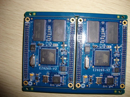
The resistance is represented by "R" in the circuit, such as: R1 represents a resistance number 1. The main role of resistance in the circuit is Diversion, current limit, pressure, bias, etc. 1. Parameter recognition: The unit of the resistance is Om (ω), the multiplier unit is: thousands of Euros (KΩ), Mago (MΩ), etc. Convert The method is: 1 trillion Euros = 1000,000 Euros = 1000000 Euros There are three types of parameter marking methods of the resistance, namely the direct marking method, the color standard method and the number of the number. A. The number of bidding methods is mainly used for small -volume circuits such as patch, such as: 472 represents 47 × 100Ω (ie 4.7K); 104 means 100K B. The color ring labeling method is used most most. Four -color ring resistance five -color ring resistance (precision resistance) 2. The relationship between the position and magnification of the resistance of the resistor is shown in the table below: Color valid digital multiplier
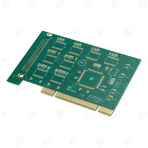
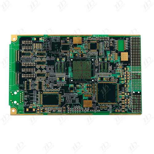
Base / thickness: FR-4 / 1.2mm Size: 140mm*159mm Minimum line width / line distance: 6mil / 6mil Minimum Pores: 0.4mm Surface treatment: Electro -plated File format: Gerber Category: Computer; Four Floor Base / thickness: FR-4 / 1.6mm Size: 294mm*200mm Minimum line width / line distance: 5mil / 5mil Minimum Pores: 0.3mm Surface treatment: tin spray (hot wind flat)
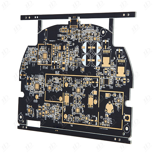
Generally speaking, the four -layer circuit board can be divided into top, bottom, and two middle layers. On the top and the bottom layer, the middle layer first uses Add Plane to add internal Plane1 and Internet Plane2 to the most power layer such as VCC and stratum (that is, the corresponding network labels are connected to the corresponding network label with ADD Plane Do not use Add Layer, this will increase the Midplayer, which is mainly used as a multi -layer signal line placement), so that Plnne1 and Plane2 are two layers of copper leather connected to the power VCC and ground GND. If there are multiple power supplies such as VCC2 or strata such as GND2, first use a thick wire or fill the Fill in Plane1 or Plane2 (at this time the bronze skin corresponding to the corresponding copper or the corresponding of Fill does not exist. You can clearly see the wire or obviously see the wire or you can clearly see the wire or the light or the light or Fill) The rough area of the power
Analysis of tin and sulfuric acid before work. Each 100m2 plate is required to add 11L sulfuric acid, 600 g Tin Salt 235, 600 mlsulfotech part A, 800 ml Sulfotech Part B, 750ml STH Additive Sulfolyt. Automatically add 56ml Sulfotech Part A at 200AH. The solution must be conducted every week to observe and adjust the Sulfotech Part A, Sulfotech Part B. The best value of the project SN2+ 20-30 ml/L 24ml/L W (H2SO4) is 98% 160-185ml/L 175ml/L/L Sulfotech Part A) 30-60ml/L 40ml/L) STH (STH Additive Sulfolyt) 30-80ml/L 40ml/L Sulfotech Part B) 15-25ml/L 20ml/L Operating temperature 18-25 ° C 22 ° C Cathode current density 1.3-2.asd 1.7asd [2]
1 process process The printed board of the graphic plate → acid oil removal → scanning water washing → secondary countercurrent water washing → micro -erosion → scanning water washing → secondary countercurrent water washing → copper plating pre -immersing → copper plating → scanning water washing → pre -immersion of tin plating → Tin -plated → III countercurrent water washing → lower panel 2 Detailed process process 2.1 Tin -plated pre -immersion 2.1.1 Composition and operating conditions of tin -plated pre -immersion fluid 2.1.2 The cylinder method of pre -immersing tin -plated groove Add half -cylinder distilled water first, then slowly immerse the 15L mass score of 98%, stir and cool down, add 1.5L Sulfotech Part A, stir well, add distilled water to 300L and stir well to use it. 2.1.3 The maintenance and control of tin -plated pre -immersed groove liquid Each treatment of 100m2 plates requires 1L sulfuric acid and 100mlsulfotech part A. Whenever the slot is treated with
High -speed PCB design rules are usually divided into two types: physical rules and electrical rules. The so -called physical rules refer to some design rules based on physical dimensions. For example, the line width is 4mi1, the distance between the line is 4mi1, and the length of the parallel wiring is 4mi1. The electrical rule refers to the design rules related to electrical characteristics or electrical performance, such as wiring delay control between INS and 2NS, and the total amount of stringing on a certain PCB line is less than 70mV. Define the physical rules and electrical rules to further explore high -speed wiring. High -speed wirms based on physical rules (physical rules) include AutoActive RENers, CCT wiring, B1AZEROUTER wiring, and Router Editor wiring. In fact, these wiringers are automatic wiring drivers of physical rules, which is It is said that these roders can only automatically meet the requirements of the physical dimensions specified by the design engineer,

Digital systems have strict requirements for timing. In order to meet the requirements of the signal timing, adjustment of the signal wiring on the PCB has become part of the PCB design work. Adjusting the wiring length includes two aspects: relative and absolute. The so -called relative is that the length of the wiring is consistent, and ensure that the signal is synchronized to several receivers. Sometimes there is correlation between a set of signal lines on PCB. For example, the bus needs to be corrected, because the signal needs to be synchronized at the receiving end. Its adjustment method is to find out the longest wiring, and then adjust other wiring to the equal length. The absolute requirement is to control the delay of the wiring between the two devices to a certain value, such as the delay between the device A and B as the ins, and this requirement is often proposed by the high -speed circuit designer, and the PCB engineer will realize it. Essence To meet this require
PCB multi -layer board refers to the multi -layer line board used in electrical products. The multi -layer board uses more single -panel or double panel wiring board. Use one double -sided as the inner layer, two -sided single -sided as the outer layer or two double -sides as the inner layer, two -sided single -sided outer layer printing line board, alternate the positioning system and insulating bonding material, and the electrophoretic graphics The interconnected printing circuit boards are made according to design requirements. With the continuous development of SMT (surface installation technology) and the continuous launch of the new generation of SMD (surface installation device), such as QFP, QFN, CSP, BGA (especially MBGA), make electronic products more intelligent and miniaturized, so Promote major reforms and progress of PCB industry technology. Since IBM first successfully developed high -density and multi -layer boards (SLC) in 1991, major groups from various countries
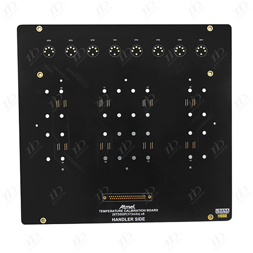
Since the mid -1980s in the mid -1980s, its output value and production have increased at a rate of more than 10 % (compared with the previous year). Because the components develop rapidly to `light, thin, short, small" " Multi -layer boards will be the most influential and vitality door category in the printing circuit board industry, and become the leading product. The multi -layer plate structure will move towards diversified and thin -level high -level, while the M C m one L structure will be faster faster. Development. Multi -layer board requires high device and technology investment. In the future, high -level multi -layer boards will be concentrated in strong PC B large manufacturers to develop and produce High density Thin, high (high) layered Diversity of multi -layer plate structures The thin substrate of the high -performance thin copper box High flatness and surface coating technology of the board surface Dead multi -layer board and rigidity multi -layer board
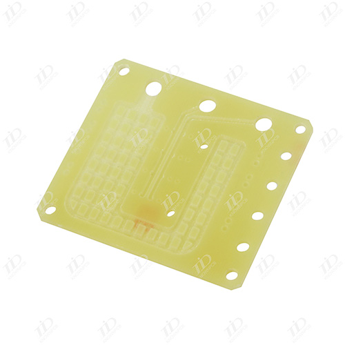
Any printing board has the problem of assembly with other structural parts. Therefore, the shape and size of the printed board must be based on the structure of the product [5]. However, from the perspective of production technology, it should be as simple as possible. Generally, it is a rectangular shape that is not very different in length and width to facilitate assembly, improve production efficiency, and reduce labor costs. In terms of number of layers, it must be determined according to the requirements of the circuit performance, the size of the board, and the density of the circuit. For multi -layer printing boards, the application of four -layer board and six -layer board is the most widely used. Taking four layers of boards as an example, the two wire layers (component surface and welding surface), a power layer, and a formation. Each layer of the multi -layer board should be symmetrical, and it is best to count the bronze layer, that is, four, six, and eight layers. Be
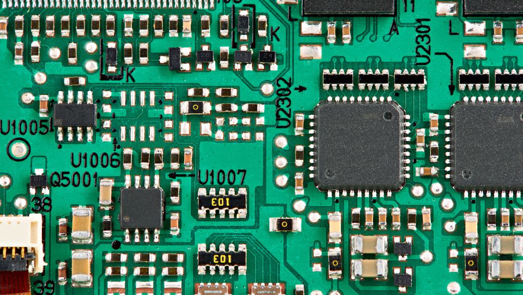
1. The MeChanical mechanical layer, as its name implies, is used for mechanical molding, that is, the appearance of the entire PCB. In fact, when we talk about the mechanical layer, we refer to the appearance structure of the entire PCB circuit board. It can also be used to set up the shape size, data mark, alignment mark, assembly description and other mechanical information of the circuit board. The information changes according to the requirements of the design company or PCB manufacturer. In addition, the Mechanical layer can be connected to other layers to output together. 2. Keep Out Layer (forbidden wiring layer), which is used to define components and wiring areas that can be effectively placed on the circuit board. Draw a closed area as an effective area for wiring. It cannot be automatically deployed and wiring outside this area. When we lay a copper with electrical characteristics, the wiring layer is prohibited from defining the boundary, that is, after we first define
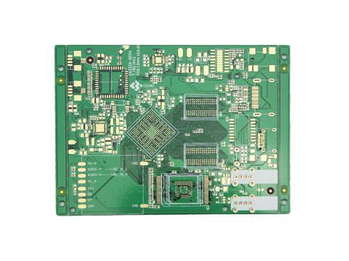
When pressing, PP and copper foil are added on both sides of the double panel, and the high temperature and high pressure are pressed into a multi -layer board. In short, the four -layer board has an inner layer. In terms of process, some circuits will be carved and suppressed in the inner layer. Double -panels can directly cut out the drilling of the factory board. The four -layer board refers to the printing circuit board. PCB is made of four -layer glass fiber, which can reduce the cost of PCB, but the efficiency is very low. Although it is difficult to get the four -layer PCB board by observing the cross section of PCB, few people have such vision. However, you can identify the four -layer board by observing the guide hole. If the same guide hole, or the motherboard or the graphics card can be found on both sides of the PCB, if the position of the guide hole cannot be transmitted, it is a four -layer board. The four -layer circuit board is made of combination on the basis of

processing method: The processing process of PCB factory similar to epoxy resin/glass woven fabric (FR4), but the board is relatively crispy and easy to break the board. Drilling and gong knife life should be reduced by 20%during drilling and gongs. 2. PTFE (polytetrafluoroethylene) material processing method: 1. Open ingredients: The protective film must be kept to prevent scratching and indentation 2. Drilling: 2.1 Use a new drilling (standard 130), the best one by one, the pressure of the feet is 40PSI 2.2 Aluminum sheet is a cover, and then use a 1mm mighty pad to step up the PTFE board 2.3 After drilling, use a wind gun to blow out the dust in the hole 2.4 Use the most stable drill, drilling parameters (basically the smaller the hole, the fast drill speed, the smaller the chip load, the smaller the return speed) 3. Pole treatment 3. Pole treatment Plasma treatment or sodium cricket activation treatment is conducive to hole metalization 4. Pth Shen copper 4.1 Afte
1. The odd number layer PCB needs to add non -standard layer of core layer bonding process on the basis of the core structure process. Compared with nuclear structures, the production efficiency of the PCB circuit board processing plant with foils outside the nuclear structure will be reduced. Before layer pressing, the outer core needs additional process processing, which will increase the risk of scratching and etching errors. 2. A balanced structure Avoid bending. The best reason for the design without a strange layer of PCB is that the strange layer of the circuit board is easy to bend. After the multi -layer circuit key combination process is completed, when the PCB is cooled, different layer of pressure tension will cause PCB to bend when the core structure and foil structure cool. As the thickness of the circuit board increases, the risk of curvage of two different structures of composite PCB is greater. The key to eliminating circuit boards is to use balanced layers. Altho
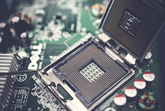
1 layer pressure The layer pressure parameters may be different because the plates of different companies may be different. Take the Shengyi substrate and PP as a multi-layer board mentioned above, in order to ensure the full flow of the resin, make the combination of good combination, and require lower the heating rate (1.0-1.5 ° C / min) and multi-paragraph The pressure is coordinated, and the time is required for a long time during the high temperature stage, and 180 ° C is maintained for more than 50 minutes. Here are the recommended sets of boarding program settings and the actual heating of the plate. The binding force of the pressed plate to detect its copper foil and the substrate is 1.ON / MM. The plates after the picture have no layering and bubbles after six thermal shocks. 2 drilling processing Drilling conditions are an important parameter that directly affects the quality of the hole wall of PCB during processing. Because the halogen -free copper plate is used to i

In terms of the principle of halogen -free base boards, most of the halogen -free materials are mainly phosphorus and phosphorus nitrogen. When the phosphorus resin is burned, it is heated to generate polymer phosphoric acid, which is extremely dehydrated. The surface of the high -molecular resin forms a charcoal film. The resin combustion surface contacts the air to extinguish the fire and achieve the flame retardant effect. Polymer resin containing phosphorus nitride compounds produce non -combustible gases during combustion to help the resin system flame retardant. The halogen-free substrate materials are based on the JPCA-ES-01-2003 standard: the copper-covering plate with a chlorine (C1) and bromine (br) content of less than 0.09 % WT, respectively, is defined as a halogen-free copper plate. (At the same time, the total amount of CI+BR ≤0.15 % [1500ppm]). Why do halogen refers to the halogen elements in the chemical element cycle table, including fluoride (F), chlorine (CL),
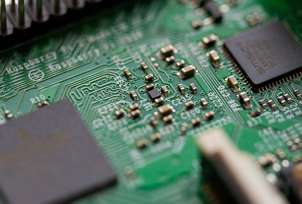
1. Line and Pattern (Pattern): The line is a tool for turning between the original. In the design, the design will be designed as a large copper surface as the ground and power layer. The lines and the diagram are made at the same time. 2. Throughhole/VIA: The guide holes can turn the lines above two levels of lines, and the larger guide holes are used as parts plug -in. Putting and positioning, fixed screws during assembly. Industrial control circuit board 3. SolderResistantant/SolderMask: Not all copper noodles have to eat tin parts, so it will printed a layer of substances from copper noodles (usually epoxy resin) to avoid Non -short circuit between the lines of tin. According to different processes, it is divided into green oil, red oil, and blue oil. 4. Dielectric: It is used to maintain the insulation between lines and layers, commonly known as substrate. 5. Legend/Marking/Silkscreen: This is a non -necessary composition. The main function is to mark the names and positi
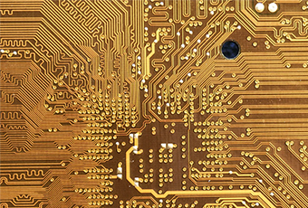
With the continuous expansion of the company's scale, the original company's website has been far from enough...HDI (High Density Interconnect Board) is a compact circuit board designed specifically for small capacity users. Compared to ordinary PCBs, the most significant feature of HDI is its high wiring density, which is mainly reflected in the following four aspects.1、HDI is smaller and lighterThe HDI board is made of the traditional double-sided board as the core board through continuous lamination. This kind of circuit board made by continuous layering is also called build-up multilayer board (Build-up Multilayer, BUM). Compared with traditional circuit boards, HDI circuit boards have the advantages of "light, thin, short, and small".The electrical interconnection between HDI board layers is realized through conductive through holes, buried holes and blind holes. Its structure is different from ordinary multilayer circuit boards. A large number of micro-buried blind holes
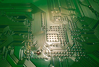
You may always hear about core and prepreg in PCB production. The material is composed of copper foil, reinforcement, resin matrix, and filler system. And each part plays a key role.The appropriate materials have a good quality assurance for the products that produced, but it's not that the more expensive the material is, the more suitable it is for your products.Please kindly contact us KnownPCB, we can provide a variety of material for your better choice.
Inquiry Now

