 +86 755 2794 4155
  sales@knownpcb.com
-
Shenzhen KNOWNPCB Technology Co., Ltd.
 +86 755 2794 4155
  sales@knownpcb.com
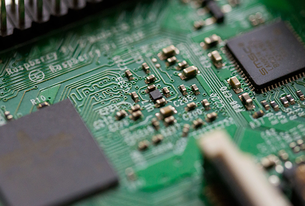
Have you noticed that now more and more of our lighting is using led lighting.What is LED? Compared to the traditional light bulbs, LEDs have lower power consumption, longer lifetime and higher energy efficiency. In the PCB industry,when we say LED PCB, it refers to the pcb used for LED lighting, if you are looking for a suitable LED PCB for your lighting system, this article may bring you something. WHAT ARE LEDS COMPOSED OF?LED is an initial light-emitting diode that produces light when an electric current passes through. LEDs typically have negative and positive electrodes, which generate light in the visible light region.The LEDS are glued to the PCB by soldering process and have electrical connections for lighting.Since light-emitting diodes dissipate a lot of heat when they are in use, when you are designing LED, the metal core is usually the best choice for LED PCB, it is because that it dissipates heat more faster. Among them, the metal material aluminum is the most widely used
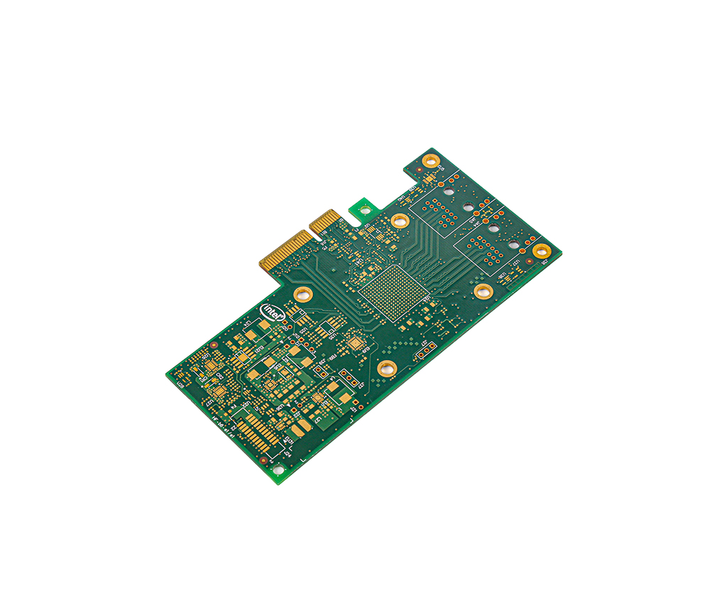
The global PCB industry accounts for more than a quarter of the total output value of the electronic component industry, and is the industry with the largest proportion among various electronic component sub industries, with an industry scale of 40 billion US dollars. Meanwhile, due to its unique position in the electronic basic industry, it has become the most active industry in the contemporary electronic component industry. In 2003 and 2004, the global PCB output value was 34.4 billion US dollars and 40.1 billion US dollars, with year-on-year growth rates of 5.27% and 16.47%, respectively. Development status of domestic PCB industry The PCB development work in China began in 1956 and gradually expanded to form the PCB industry from 1963 to 1978. After more than 20 years of reform and opening up, due to the introduction of advanced foreign technology and equipment, single panel, double-sided board, and multi-layer board have all achieved rapid development, and the domestic PCB i
In the early years, circuit boards belonged to the high-tech industry, and most foreign companies controlled technology output, which at one time constrained and restricted the development and growth of the circuit board industry. According to Time magazine, China and India are among the most polluted countries in the world. To protect the environment, the Chinese government has been strictly formulating and implementing relevant pollution control regulations, which have affected the PCB industry. Many cities and towns are no longer allowed to expand and build new PCB factories, but the development of our circuit board enterprises is now restricted by local conditions. The more economically developed the areas, the greater the restrictions. Why? Because unconsciously, circuit board enterprises have developed into what the government sees as major polluters, energy consumers, and water users! In today's society where environmental protection and sustainable development are highly va
Frequently Asked Questions 1、 Degreasing (temperature 60-65 ℃) 1. Too much foam: abnormal quality caused by too much foam: poor degreasing effect, caused by mismatched bath solution. 2. Composition of particulate matter: The reason for the composition of particulate matter is that the filter is broken, the high-pressure water washing of the grinding machine is insufficient, and dust is brought in from the outside. 3. Finger prints cannot be degreased: Finger prints cannot be degreased due to low degreasing temperature and incorrect dispensing of medication. 2、 Micro corrosion (NPS 80-120G/L H2SO4 5% temperature 25-35 ℃) 1. The copper surface of the board is slightly white: the reason is due to insufficient grinding, oil removal, or contamination, and low concentration of liquid medicine. 2. The copper surface of the board is black: it cannot be washed clean after oil removal and is contaminated by oil removal. A pink surface on copper indicates a normal effect of micro etchi

1. Copper foil is excessively etched, and the electrolytic copper foil used in the market is generally single-sided galvanized (commonly known as ashed foil) and single-sided copper plated (commonly known as reddened foil). The common copper throwing is generally galvanized copper foil above 70um, while reddened foil and ashed foil below 18um have not undergone bulk copper throwing. 2. Local collisions occurred during the PCB process, causing the copper wire to detach from the substrate due to external mechanical forces. This defect manifests as poor positioning or directionality, where the detached copper wire will have obvious twisting or scratches/impact marks in the same direction. Peel off the defective copper wire and observe the rough surface of the copper foil. It can be seen that the color of the rough surface of the copper foil is normal, and there will be no side corrosion defects. The peeling strength of the copper foil is normal. 3. Unreasonable PCB circuit design, u

1. Engineering design: The arrangement of interlayer semi cured sheets should correspond; Multi layer core boards and semi cured sheets should use the same supplier's products; The outer C/S surface graphics area should be as close as possible, and independent grids can be used; 2. Drying board before cutting Generally, at 150 degrees Celsius for 6-10 hours, the moisture inside the board is removed, further allowing the resin to cure completely and eliminating stress inside the board; Drying the board before opening, both the inner layer and both sides are required! 3. Before laminating the multi-layer board, attention should be paid to the longitudinal and latitudinal directions of the cured sheet: The shrinkage ratio in the warp and weft directions is different, so pay attention to distinguishing the warp and weft directions before cutting and stacking the semi cured sheet; When cutting the core board, attention should also be paid to the warp and weft directions; The gener
The equipment used for curing plastic melt ink is not suitable for curing water-based ink. Except for discharge ink, other water-based inks contain chemical cross-linking agents. Only when water-based inks are sufficiently dried can they ensure the washing fastness of printed images. Some printing factories choose air drying for the solidification of water-based ink, while others make the printed matter come into direct contact with a hot platform before the ink dries, causing the moisture to evaporate, and then place the printed matter in an oven. Before coating the paper, a drying device should be used to remove moisture from the paper, which is also suitable for removing moisture from water-based inks. Perhaps the most reasonable way to remove moisture is to avoid adding water to the printing process. Therefore, if it is possible to print transparency on light or white fabrics Ink, which means using fine screen printing transparent ink, will have very little moisture.
(1) One point grounding Concentrate several grounding points of the same level unit circuit as much as possible to avoid the AC signal from other circuits from entering the same level or from the AC signal in the same level from entering other circuits. Suitable for low-frequency circuits with a working frequency of less than 1MHz. If a single point grounding is used when the working frequency is between 1-1OMHz, the length of the ground wire should not exceed 1/20 of the wavelength. In short, single point grounding is the basic principle for eliminating common impedance interference of the ground wire. (2) Multiple grounding points nearby There are a large number of common ground wires distributed at the edges of the PCB and present a semi closed circuit (anti magnetic field interference). All levels of circuits are grounded nearby to prevent the ground wires from being too long. Suitable for high-frequency circuits with signal operating frequencies greater than lOMHz. (3) Groun
Mechanical characteristics of PCB through holes When the PCB through-hole is large, our wiring space will be very small. Obviously, we want to use small PCB through-holes, but how small is appropriate? Even if the PCB plate making via is already very small and the PCB plate making via is smaller, more lines can be laid on the PCB to improve the wiring density. For products with limited product size, designers have to make the PCB through holes on the board smaller and smaller. The smaller the PCB through hole, the smaller the parasitic capacitance. This means that the smaller the PCB through hole, the better it will work in high-speed situations. In the fastest PCB design, small PCB through holes are mandatory. Of course, the cost of generating small PCB through holes is higher. In engineering design, it is inevitable that the higher the performance, the higher the cost, and PCB through holes are no exception. At present, we have three principles for PCB through holes: Small PCB th
PCB process PK: tin spraying vs gold plating vs gold deposition Gold plate and gilded plate are commonly used processes in the production of circuit boards nowadays, and many people are unable to correctly distinguish the differences between the two. Some even believe that there is no difference between the two, but in fact, they are not. Usually, when people choose gold plating, what is gold plating? When we refer to whole plate gold plating, we generally refer to "electroplated gold", "electroplated nickel gold plate", "electrolytic gold", "electroplated gold", "electroplated nickel gold plate". There is a distinction between soft gold and hard gold (usually hard gold is used for gold fingers), and the principle is to dissolve nickel and gold (commonly known as gold salt) in chemical solution, Immerse the circuit board in an electroplating cylinder and apply current to generate a nickel gold coating on the copper foil surface of the circuit board. Electroplated nickel gold is wide
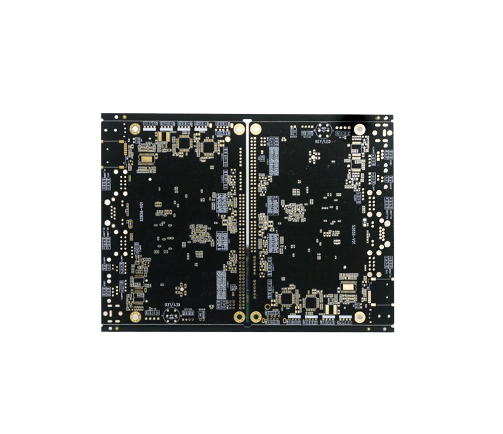
The difference between PCB tin spraying and PCB tin plating The cost of PCB solder board is relatively low because it only sprays tin on the PCB on the solder pad, while tin plating includes tin on the circuit as well. PCB tin plating, as the name suggests, is the process of depositing a thin layer of tin at the PCB pad location using chemical methods, usually ranging from 10 to 30 microns. The main purpose is to prevent oxidation and better fuse SMT tin. In fact, the same purpose as gold plating and OSP requires additional tin plating during SMT. PCB tin spraying refers to the physical method of spraying a layer of tin, usually ranging from 50 to 150 microns in thickness, which is relatively thick. Do not apply tin during SMT, just melt the tin onto the component. The composition of the two types of tin must be different. PCB based tin uses a salt of tin, and the mixture is an acidic solution containing tin. But PCB tin spraying generally uses tin alloys, which are generally divide
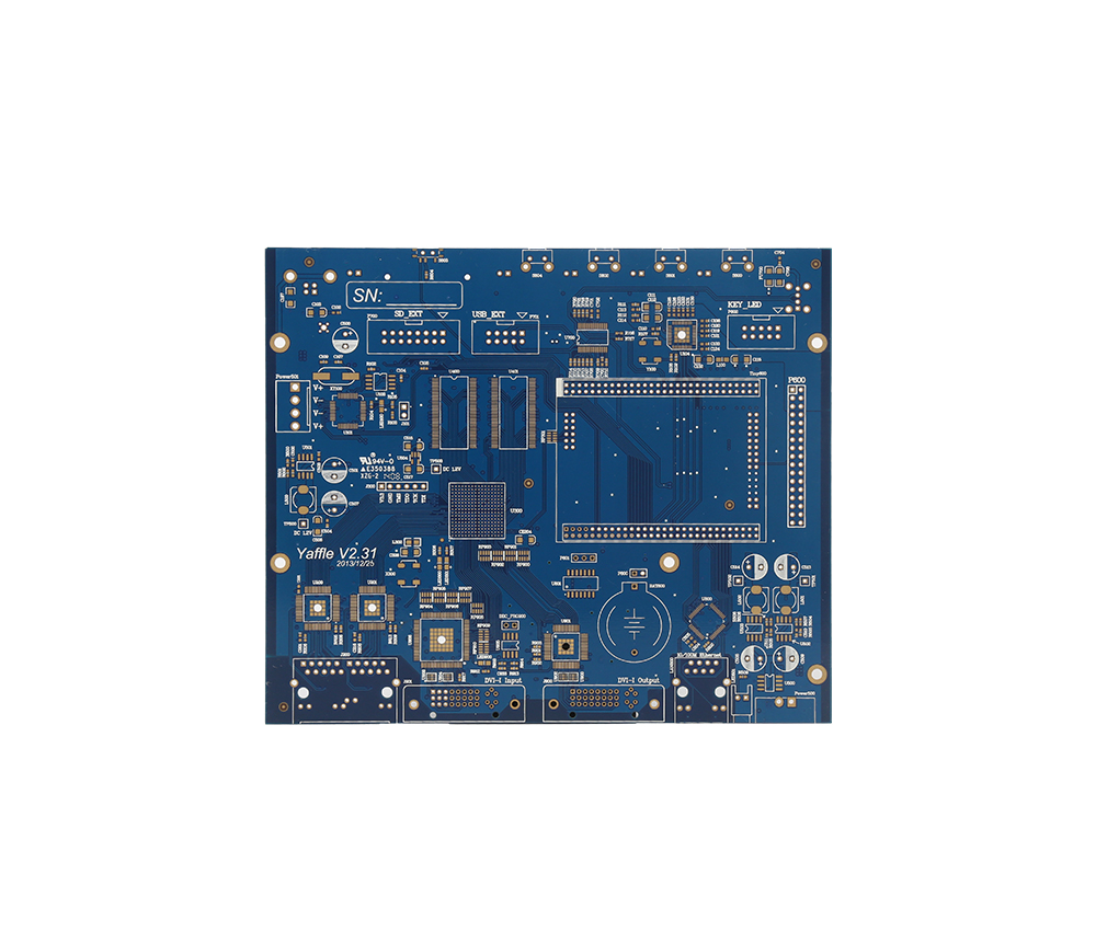
Reasons and Preventive Measures for Poor PCB Surface Mount Welding 1、 Poor wetting Poor wetting refers to the welding process where the solder and PCB substrate welding area, after being soaked, do not generate metal to metal reactions, resulting in missed or missing solder faults. The reason for this is mostly due to the surface contamination of the welding area, or the adhesion of solder resist, or the formation of a metal compound layer on the surface of the joint, such as the presence of sulfides on the surface of silver and oxides on the surface of tin, which can cause poor wetting. In addition, when the residual aluminum, zinc, cadmium, etc. in the solder exceeds 0.005%, the wetting effect of the solder reduces the activity and can also lead to poor wetting. In wave soldering, if there is gas present on the surface of the PCB substrate, this fault is also prone to occur. Therefore, in addition to implementing appropriate welding processes, anti fouling measures should be take
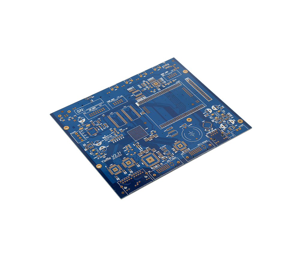
The automotive electronics market is the third largest application field for PCBs after computers and communication. With the gradual evolution and development of automobiles from traditional mechanical products to intelligent, information-based, mechatronics high-tech products, electronic technology has been widely used in automobiles, and electronic products have been used without exception in engine systems, chassis systems, safety systems, information systems, vehicle Internal environment systems, etc. The automotive market has clearly become another highlight of the electronic consumer market, and the development of automotive electronics has naturally driven the development of automotive PCBs. Among the key application objects of PCB today, automotive PCBs occupy an important position. However, due to the special working environment, safety, and high current requirements of automobiles, they have high requirements for the reliability and environmental adaptability of PCBs, and
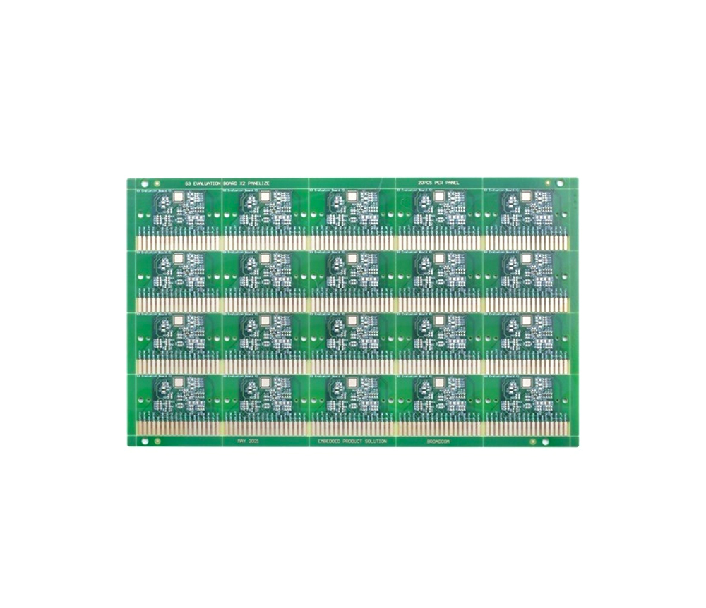
The ion transport caused by electrostatic force in electroplating solution is called ion migration. The migration rate is expressed as follows: u=zeoE/6 π r η Yes. Where u is the ion migration rate, z is the charge number of the ion, and eo is the charge amount of one electron (i.e. 1.61019CE is the potential, r is the radius of the hydrated ion η Is the viscosity of the electroplating solution. According to the calculation of the equation, it can be seen that under the action of the electric field. The greater the decrease in potential E, the smaller the viscosity of the electroplating solution, and the faster the rate of ion migration. When electroplating, according to the theory of electrodeposition. The PCB located on the cathode is a non ideal polarized electrode. Copper ions adsorbed on the surface of the cathode obtain electrons and are reduced to copper atoms, resulting in a decrease in the concentration of copper ions near the cathode. Therefore, a copper ion concentratio
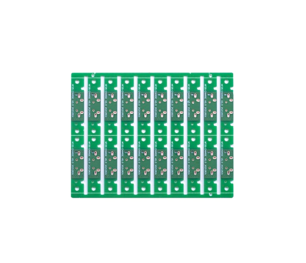
Anime image measuring instrument is applicable to all application fields aiming at two-dimensional measurement, and is widely used in machinery, electronics, instruments, hardware, plastics and other industries. Anime image measuring instrument (also known as image mapping instrument) is based on CCD digital image, relying on computer screen measurement technology and powerful software capabilities of spatial geometry operation. After installing specialized control and graphic measurement software, the computer becomes the measurement brain with the soul of the software and is the main body of the entire device. It can quickly read the displacement value of the optical ruler, and through software module operations based on spatial geometry, instantly obtain the desired results and generate graphics on the screen for the operator to compare the images, thus intuitively distinguishing possible deviations in the measurement results. All of this is done in real-time in front of today
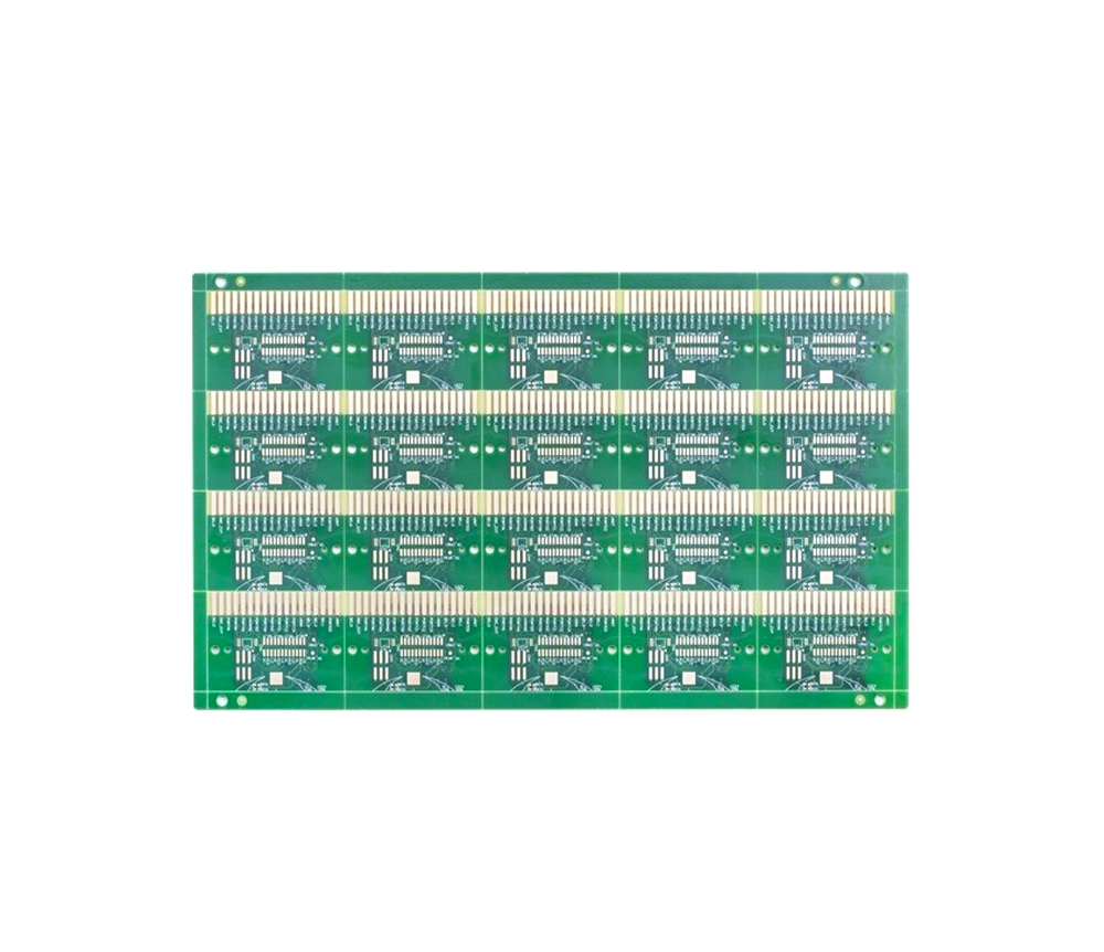
Symptom: There are blasting holes in the cold or solder joints. Inspection method: Conduct regular analysis of the holes before and after immersion welding to identify areas where copper is under stress. In addition, perform incoming inspection on raw materials. Possible reasons: 1. Explosion holes or cold solder joints are seen after soldering operations. In many cases, poor copper plating can lead to expansion during soldering operations, resulting in cavities or explosive holes on the wall of the metallized hole. If this is generated during the wet processing process, the absorbed volatilization The object is covered up by the coating and then driven out under the heating effect of immersion welding, which will create a nozzle or blasting hole. Solution: 1. Try to eliminate copper stress. The expansion of laminates in the z-axis or thickness direction is usually related to the material. It can promote the fracture of metallized pores. Dealing with laminate manufacturers to
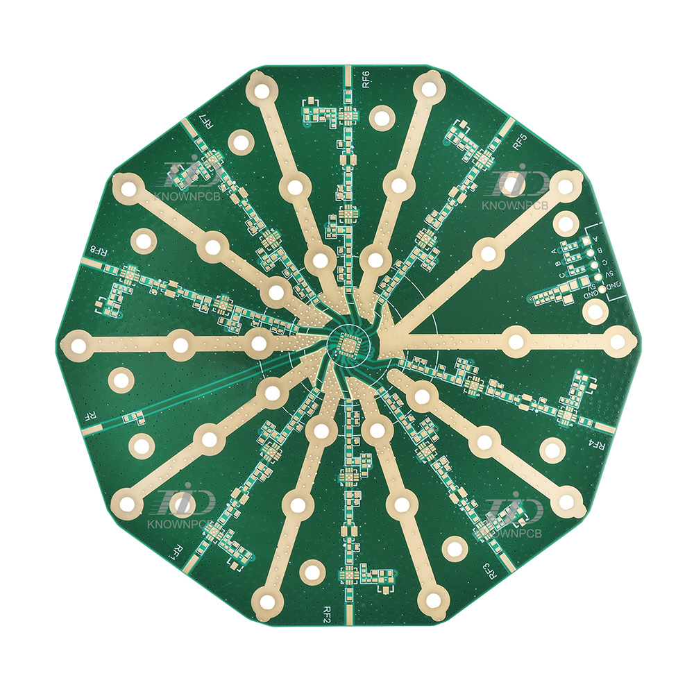
1、 Bridging The causes of bridging are mostly due to excessive solder or severe edge collapse after solder printing, or excessive PCB substrate solder area size, SMD mounting offset, etc. During the refinement stage of SOP and QFP circuits, bridging can cause electrical short circuits and affect product use. 2、 Poor wetting Poor wetting refers to the welding process where the solder and PCB substrate welding area, after being soaked, do not generate metal to metal reactions, resulting in missed or missing solder faults. The reason for this is mostly due to the surface contamination of the welding area, or the adhesion of solder resist, or the formation of a metal compound layer on the surface of the joint, such as the presence of sulfides on the surface of silver and oxides on the surface of tin, which can cause poor wetting. In addition, when the residual aluminum, zinc, cadmium, etc. in the solder exceeds 0.005%, the wetting effect of the solder reduces the activity and can al
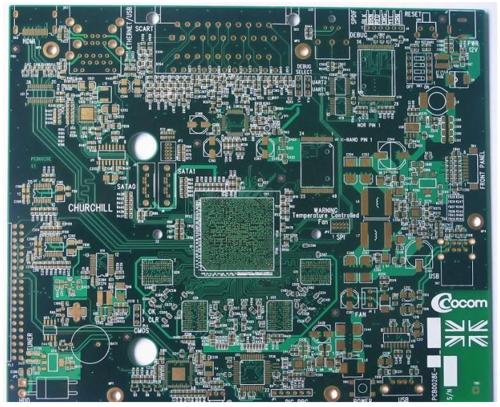
Rare metals often need to be plated on board edge connectors, protruding contacts or gold fingers to provide lower contact resistance and higher wear resistance. This technology is called finger plating or protruding part plating. Gold is often plated on the protruding contacts of nickel plated plate edge connectors. The protruding parts of the gold finger or plate edge are manually or automatically plated. Currently, the gold plating on the contact plug or gold finger has been replaced by plating, lead plating, and button plating. The process is as follows: 1) Peel off the coating to remove tin or tin lead coating from protruding contacts 2) Rinse with cleaning water 3) Scrub with abrasive 4) Activated diffusion in 10% sulfuric acid 5) Nickel plating thickness on protruding contacts is 4-5 μ M 6) Cleaning to remove mineral water 7) Gold permeation solution treatment 8) Gilding 9) Cleaning 10) Drying
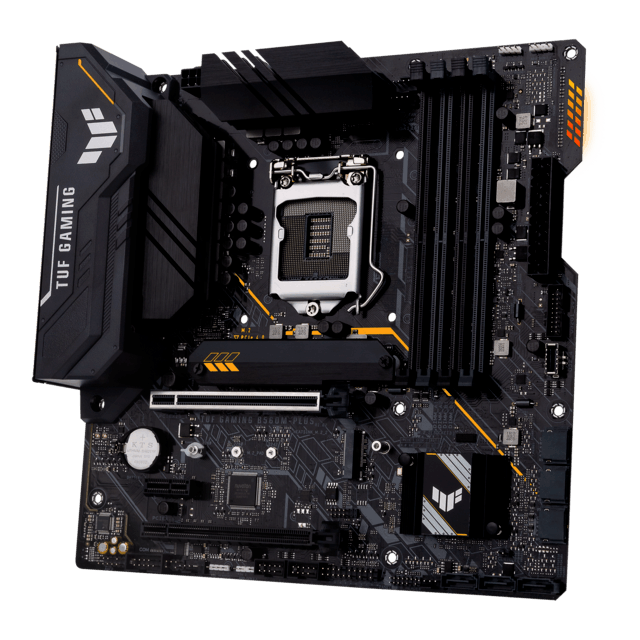
Whether the quality of PCB ink is excellent or not cannot be separated from the combination of the above major components in principle. Excellent ink quality is the comprehensive embodiment of scientific formula, progressiveness and environmental protection. This is reflected in: Viscosity is the abbreviation for dynamic viscosity. It is generally expressed in viscosity, that is, the shear stress of fluid flow divided by the Velocity gradient in the direction of the flow layer, and the International unit is Pa/s or mPa/s. In PCB production, it refers to the fluidity of ink generated by external forces. Conversion relationship of viscosity units: 1Pa. S=10P=1000mPa. S=1000CP=10dpa. s Plasticity refers to the ability of ink to maintain its pre deformation properties after being deformed by external forces. The plasticity of ink is beneficial for improving printing accuracy; Thixotropy ink is gelatinous when standing, but its viscosity changes when being touched, also known as sh
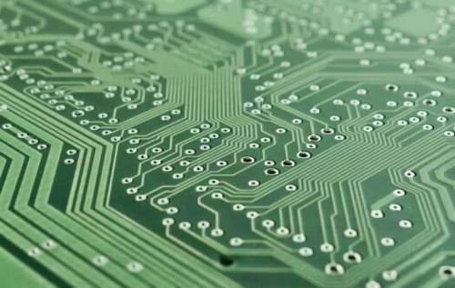
(1) Heat the waste liquid containing gold to 80-90 ℃, slowly add Iron(II) chloride solution under constant stirring, and the reaction is as follows:; Au3++3Fe2+=3Fe3++Au ↓ As the gold ions are continuously reduced, the color of the solution gradually changes from yellow to crimson, and the gold powder settles at the bottom. Continue to add excess Iron(II) oxide solution and let stand for several hours. Take two drops of static stratification solution and add two drops of 1% red blood salt. The color turns blue, indicating that the gold has been completely reduced. Pour out the upper clear liquid and filter it by vacuum method, while the lower part is precipitated with yellow gold powder. (2) Acid washing and water washing: Add a 1:2.5 hydrochloric acid solution to the gold powder and boil it, stir for 5 minutes, pour out the upper solution, and repeat this process 3-5 times until no yellow color appears. Rinse the gold powder multiple times with distilled water until the pH valu
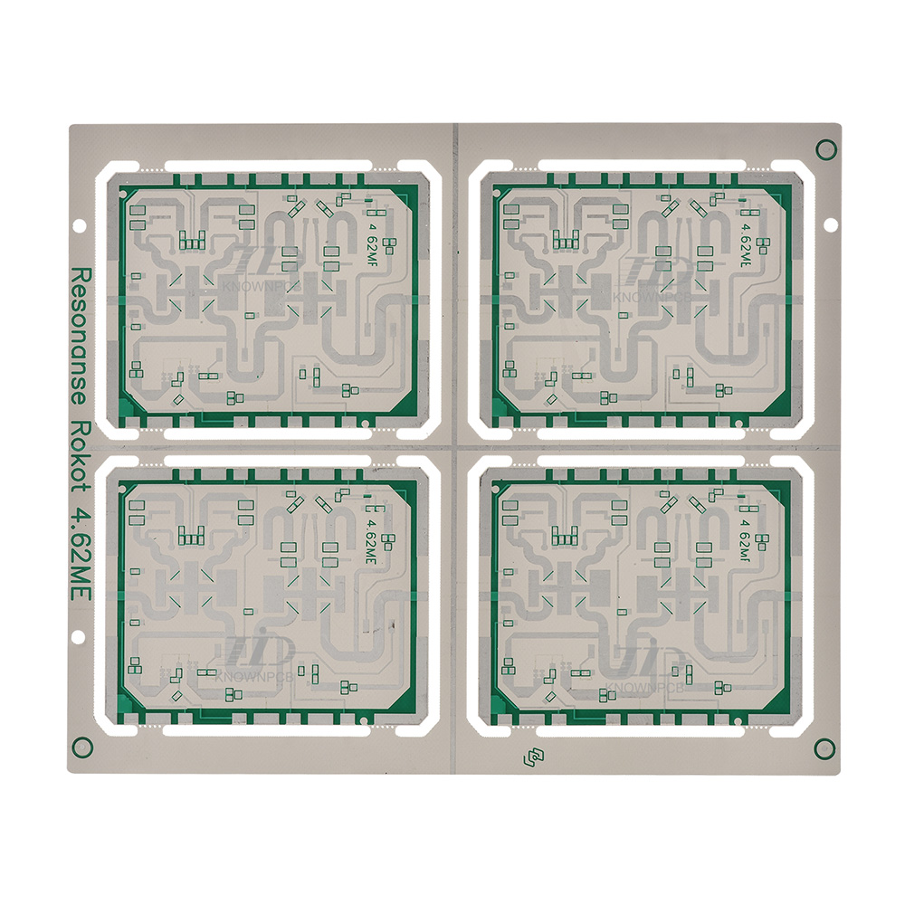
1、 Unclear definition of processing level The single panel design is on the TOP layer, and if it is not specified, it may be difficult to assemble components on the board without proper explanation. 2、 Large area copper foil too close to the outer frame The distance between the large area copper foil and the outer frame should be at least 0.2mm, as milling onto the copper foil during contour milling can easily cause the copper foil to warp and cause the solder resist to fall off. 3、 Draw solder pads with filler blocks Drawing solder pads with filler blocks can pass DRC inspection during circuit design, but it is not feasible for machining. Therefore, this type of solder pad cannot directly generate solder mask data. When applying solder mask, the filler block area will be covered by solder mask, causing difficulty in device soldering. 4、 The electrical layer is both a solder pad and a connecting wire Because the power supply is designed as a patterned solder pad, the ground
Inquiry Now

