 +86 755 2794 4155
  sales@knownpcb.com
-
Shenzhen KNOWNPCB Technology Co., Ltd.
 +86 755 2794 4155
  sales@knownpcb.com
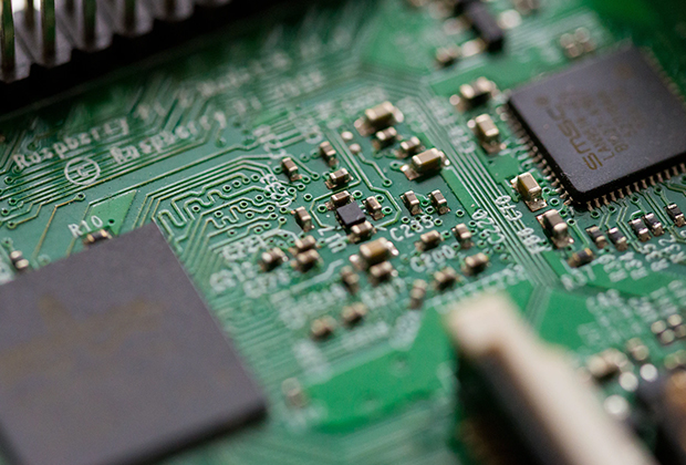
Have you noticed that now more and more of our lighting is using led lighting.What is LED? Compared to the traditional light bulbs, LEDs have lower power consumption, longer lifetime and higher energy efficiency. In the PCB industry,when we say LED PCB, it refers to the pcb used for LED lighting, if you are looking for a suitable LED PCB for your lighting system, this article may bring you something. WHAT ARE LEDS COMPOSED OF?LED is an initial light-emitting diode that produces light when an electric current passes through. LEDs typically have negative and positive electrodes, which generate light in the visible light region.The LEDS are glued to the PCB by soldering process and have electrical connections for lighting.Since light-emitting diodes dissipate a lot of heat when they are in use, when you are designing LED, the metal core is usually the best choice for LED PCB, it is because that it dissipates heat more faster. Among them, the metal material aluminum is the most widely used
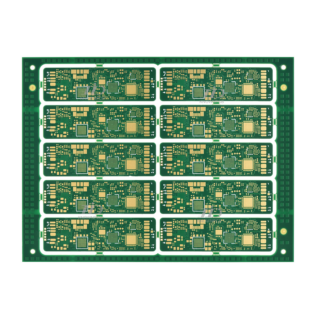
Plug -in wiring terminal The product has a needle distance of 3.5, 3.81, 5.0, 5.08, 7.5, 7.62, and 2-24. It can provide a fixed socket with screws to match and seismic connection. The plug uses the side connection technology, that is, the screw direction is perpendicular to the direction of the wire. Screw -type wiring terminal The line board wiring terminal has always occupied a very important seat in the electronics industry, and it has now become an important part of the printing line board. Its structure and design are more solid to the characteristics of screw connection that are convenient and reliable in wiring; the structure is compact, the link is reliable, and has its own advantages; the principle of lifts of the clamping body is used to ensure that the wiring is reliable and large; The body is divided into two parts to ensure that the distance when the screw is tightened will not be passed to the solder joint and damaged the welding joint; Spring -type wiring termina
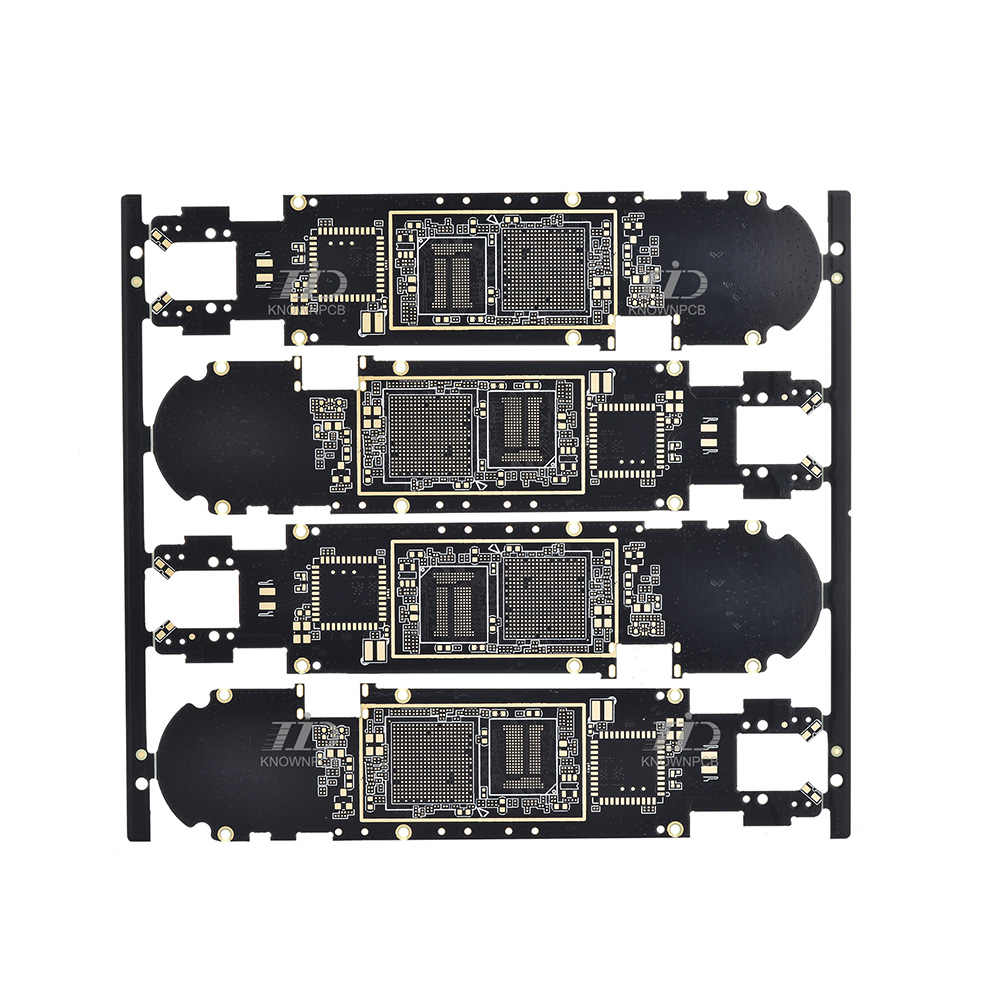
The PCB board electrical connection is the most widely used in PCB wiring terminals. How to set the height and its corresponding role in designing is. The size of the key management and control of the terminal is mainly bent terminals 1. Card point size (directly affects PIN maintenance)2. The height of the shift (directly affects the GAP value of the finished product) 3. The height of the stab (only to increase PIN maintenance, some products need) The other three aspects can be controlled 1. The chief of the terminal 2. The width of thepin feet 3. Straight lines of terminals Strengthen the control of production processes to ensure the efficient manufacturing system to ensure the quality and intersection of the product.

Flexible Printed Circuit Board (abbreviated FPC) is also known as flexible printed circuit board, or soft printed circuit board. According to the definition of IPC, the deflection of the circuit board is a product that is designed and produced by the line graphics on the deflection substrate in a printed method. (1) FPC is small and light weight. (2) FPC can move, bend, and twist. (3) FPC has excellent electrical performance, dielectric performance and heat resistance. (4) FPC has higher assembly reliability and assembly operationability. (5) FPC can be installed with three -bit connection. (6) FPC is good for heat diffusion. (7) Low cost. (8) The continuity of processing.
Number of layers of the line: single -sided FPC, double -sided FPC, multi -layer FPC Physical strength: deflection PCB, just -scratch PCB According to the substrate: polyester substrate type, organic fiber substrate type, polytexoethylene medium thin film substrate type, etc. By an enhanced layer: there is an enhanced FPC, no enhanced FPC Round density: ordinary FPC, high -density interconnection (HDI) FPC The soft plate is a printing circuit made of flexible insulating substrate, and has the advantages of many hard print circuit boards. The product volume is small, light weight, and the volume of the device is greatly reduced. The application of electronic products to high density, miniaturization, lightweight, thin, and high -reliable direction needs. , Folding, you can make a three -dimensional wiring, arbitrarily arrange according to the requirements of the spatial layout, change the shape, and move and retract in the three -dimensional space to achieve the integration of
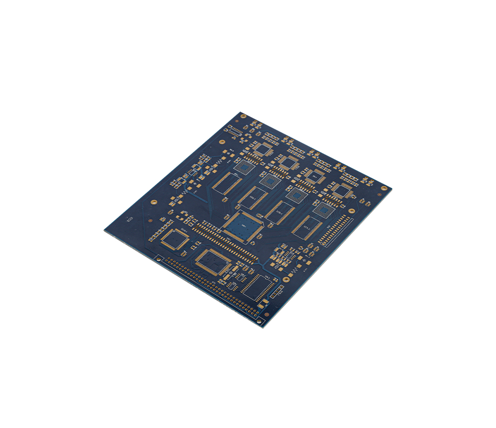
The insulation film forms the basic layer of the circuit, and the adhesive bonded the copper foil to the insulating layer. In multi -layer design, it is bonded with the inner layer. They are also used as protective coverage to separate circuits from dust and humidity, and can reduce the stress during the deflection, and copper foil forms a conductive layer. In some flexible circuits, rigid components formed by aluminum or stainless steel are used. They can provide the stability of the size, providing physical support for the resettlement of components and wires, and release of stress. Adhesives bond the rigid components and flexible circuits together. In addition, there is also a material that is sometimes used in a flexible circuit. It is a bonding layer. It is formed formed by coating on both sides of the insulating film. The bonding layer provides environmental protection and electronic insulation functions, and can eliminate a layer of film, as well as multi -layer capabilitie

During the production process, the problem of being scrapped and replenished in order to prevent too low or reduce the problem of excessive rates of drilling, pressure delay, and cutting in order to prevent too much short circuit. The best effect of the best effect is particularly important before giving birth. Pre -treatment of pre -treatment, there are three aspects that need to be dealt with. These three aspects are completed by engineers. The first is the FPC board engineering evaluation, mainly to evaluate whether the customer’s FPC board can produce, whether the company's production capacity can meet the customer's board requirements and unit costs. The supply of raw materials, in the end, the engineer processes the engineering files of the customer's CAD structure, the Gerber line data, etc. to suitable The production department and various departments such as cultural control and procurement have entered the conventional production process.
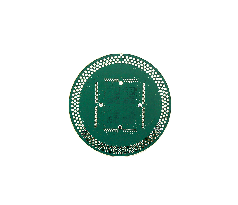
PCB production process Dual -panel system Open → Drilling → PTH → Electroplating → Pre -processing → Dry Film → Pickup → Exposure → Graph Electroplating → Dalf Meeting → Putting Dry Film → Displaying Disposal → Etancular → During Mask → Surface Treatment → Paste the cover film → suppress → curing → nickel gold → printing characters → cutting → electrical test → final inspection → packaging → shipment One -scale Open → Drilling → Patching dry film → Division → Exposure → Evidence → Decoration → Surface treatment → Patch covering film → curing → surface treatment → sinking gold → printing character → electrical test → rushing → rushing Cut → final inspection → packaging → shipment
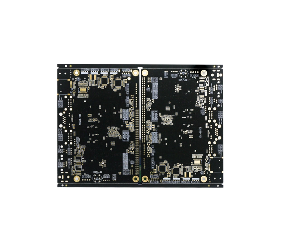
The effect of the wiring of the pad connection and the position of the pores on SMT production: The wiring of the pad connection and the position of the pores has a great impact on the welding rate of SMT, because the inappropriate pad pad connection line and the pores may play the role of "theft" solder. Walk (the rainbow suction and capacity in the fluid). The following situation is good for production quality: 1. Reduce the width of the pad connection line: If there is no current bearing capacity and limitation of PCB manufacturing dimensions, the maximum width of the pad connection line is 0.4mm or 1/2 pile width, which can be smaller. 2. The most preferably selected between the pads connected to the large -scale conductivity belt (such as ground floor, power surface) is a narrow connection line with a length of not less than 0.5mm (the width is not greater than 0.4mm or the width is not greater than 1/2). 3. Avoid introducing pads from the side or corner. The most prefera
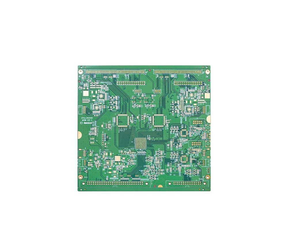
Because the production of the printed circuit board is in the second half of the electronic equipment manufacturing, it has become the downstream industry of the electronics industry. Almost all electronic equipment requires the support of the circuit board. Therefore, printing circuit boards are products with the highest market share in global electronic component products. Japan, China, Taiwan, Western Europe and the United States are the main printed circuit board manufacturing bases. Benefiting from the new products and new market support, the global PCB market has successfully achieved recovery and growth. According to the statistics of the Hong Kong Circuit Board (HKPCA), the global PCB market will develop steadily in 2011, and it is expected to grow by 6-9%, and China is expected to increase by 9-12%. The Taiwan Institute of Technology (IEK) analysis report predicts that the global PCB output value will increase by 10.36%in 2011 to US $ 41.615 billion. According to the rep

The copy plate is removed by a piece of PCB board components, and the surface is clean. We must copy it to the PCB file and follow the steps as follows: 1. Scan the top layer, save the picture, and name top.jpg. At this time, the scanning DPI can be set according to different density. If the settings are 400dpi. 2. Scan the bottom plate, save the picture, and get the name bottom.jpg 3. Make out the middle layer 1 with coarse sandpaper, leak the copper skin, clean it after cleaning, and scan the picture, and get the name MID1.JPG 4. Make the middle layer 2 with coarse sandpaper, leak the copper skin, get it clean, and scan the picture. 5. In the Photoshop, adjust each picture horizontally (select the picture to ensure that the picture is level, so that the lines that come out of this look good, and multiple pictures can be easily aligned). It is recommended to make the underlying image horizontal image in order to make the bottom diagram It is the same direction, the upper and
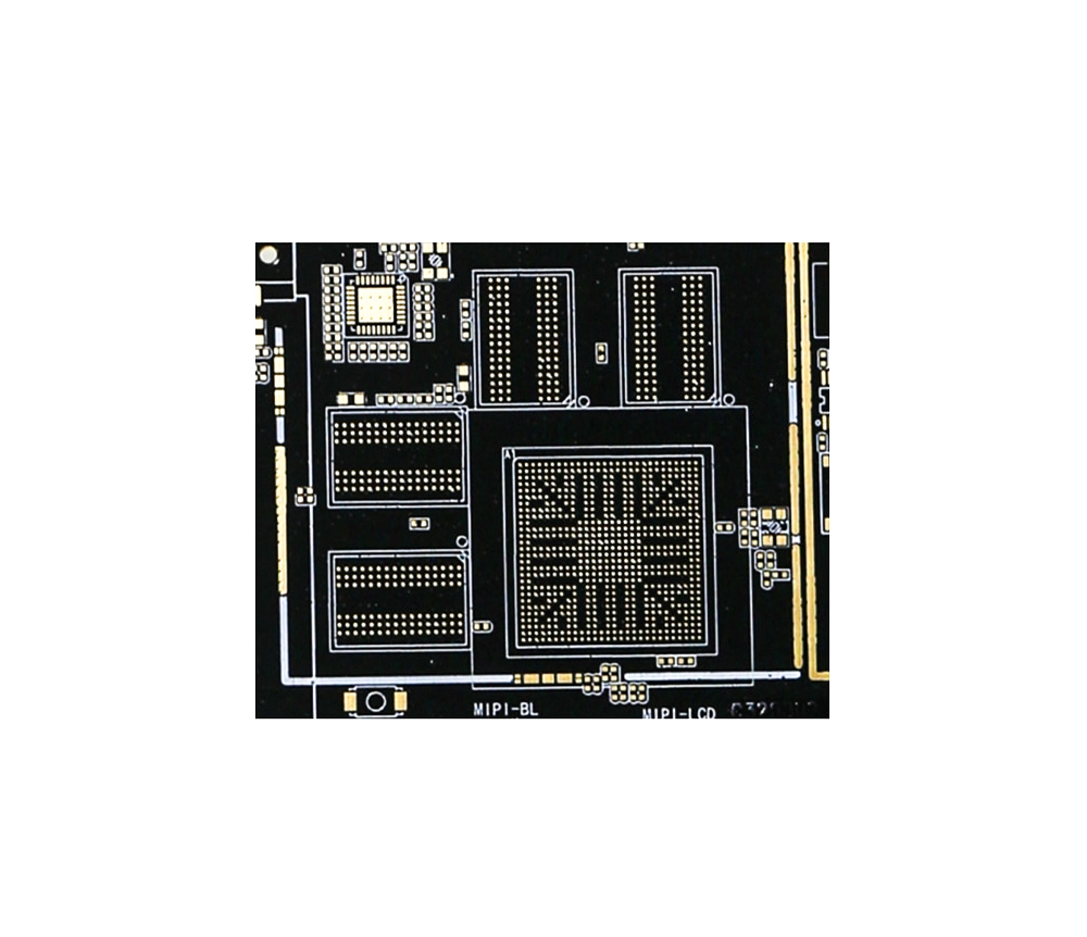
Flexible circuit board (FlexiblePrintedCircuit, FPC), also known as soft circuit board and deflection circuit board, is very popular with excellent characteristics such as light quality, thin thickness, and free bending folding ... It mainly relies on artificial visual inspection, with high cost and low efficiency. With the rapid development of the electronics industry, the design of circuit board design has become more and more high -precision and high density. Traditional artificial testing methods can no longer meet production needs. FPC defect automation testing has become an inevitable trend of industrial development. Flexible circuit (FPC) is a technology developed by the United States to develop aerospace rocket technology in the 1970s. It is a high reliability, excellent deflection made by polycatis film or polytamine as a substrate material. The printing circuit is embedded in the circuit design on the bending light and thin plastic sheet to make a large amount of precisi
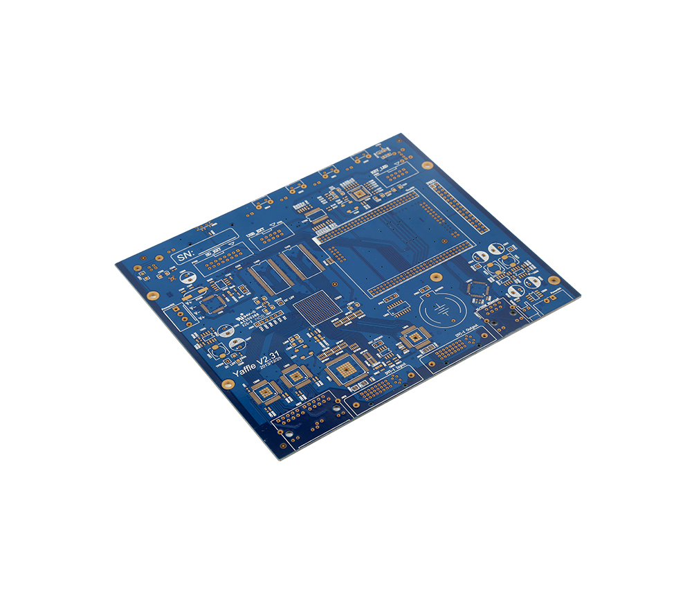
It is composed of a combination bracket, a padding combination plate, a frame support guide system, a material support frame, a unloading device, a cutting knife and its fixing device, an upper plate support system, and a cutting speed changing device. The upper surface of the combination bracket is short, and the padding combination plate is horizontally fixed on the combination bracket. There are slits corresponding to the number of cutting knives on the padding combination plate, The frame support guide system is composed of several pairs of guide sliding devices fixed on the combined bracket and several pairs of positioning devices. The guide sliding devices are fixed on both sides of the combined bracket in pairs, and the positioning devices are also fixed on both sides of the combined bracket in pairs. The material support frame is connected to the frame support guide system in a sliding manner, The guiding sliding device in the frame support and guidance system only allows t
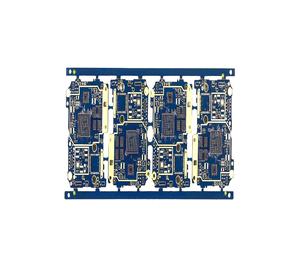
A universal circuit magic board, consisting of a circuit experimental board and circuit components, characterized in that the circuit experimental board (for the sake of specific explanation, electronic circuits are used as examples below) is composed of a double-layer single-sided (or double-sided) printed circuit board of the same size (hereinafter referred to as the printed board), circuit component sockets (such as integrated component sockets, hereinafter referred to as sockets), and pins, A socket is welded into a metalized hole in a printed circuit board that is separated and insulated between the upper and lower layers. On the upper and lower sides centered on the horizontal centerline of the socket, a horizontal line parallel to the horizontal centerline of the socket is printed on the lower layer printed circuit board (or upper layer printed circuit board), and a vertical line perpendicular to the horizontal center of the socket is printed on the upper layer printed circu
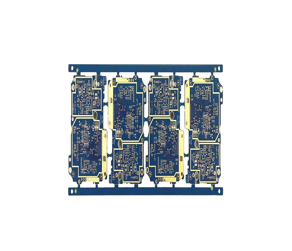
PCB board fixture is a detection device for PCB boards, especially a fixture for PCB board detection. There is a fixed seat set on the machine base that can slide back and forth, a front gear lever and a rear gear lever set on the fixed seat. The front gear lever is fixedly connected to the fixed seat, and the rear gear lever is slidably connected to the fixed seat. The front gear lever is equipped with a PCB board clamp head composed of a warping plate and a top plate, and the middle part of the PCB board clamp head is connected to the front gear lever pin, and a top rod device is set at the front end of the machine base, The top rod device is composed of a base fixed on the machine base and a top rod set on the base. When the fixed base moves to the forefront, the top rod of the top rod device contacts the top plate. The utility model has a simple structure and can conveniently and quickly clamp the PCB board, improving work efficiency. At the same time, the clamping of the PCB b
Panel length: 330mm Overall dimensions: 700 x 230 x 420 Panel thickness: 0.3-3.5 mm Machine weight 165kg 1. Fully pneumatic control, no noise 2. Small travel, less prone to product damage, and safe operation 3. Tailored work, suitable for various thicknesses of PCB 4. Minimize the internal stress generated during plate cutting to avoid tin cracking 5. The distance between the upper and lower knives can be accurately adjusted, avoiding tool loss due to different depths of the V-groove 6. The highest part at the edge of the separable V-groove is 70mm
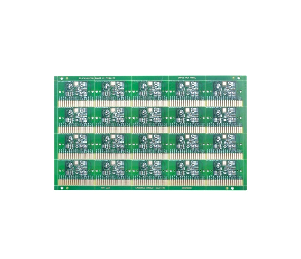
Computer and peripherals: motherboard, monitor, network card, memory card, IC, mouse, router, camera, USB drive, fan motor, game console, game card board (gold finger board) Mobile phone: mobile phone board, charger electronic anti-theft lock audio, printer, copier, fax machine, phone, scanner monitoring system, video head DV, camera meter board Automotive products: Sensors for various machines such as car audio, air conditioning switches, control system lighting fixtures, LED panels (LCD displays, LCD billboards) Bathroom equipment: motors, controllers, switches, and high-end PCB boards in industries such as medical equipment, military equipment, aerospace equipment, etc
Double-sided PCB board is a very important type of PCB board in the circuit board market. There are double-sided circuit boards with metal base, Hi Tg heavy copper foil circuit boards, flat and winding double-sided circuit boards, high-frequency PCBs, mixed dielectric base high-frequency double-sided circuit boards, etc. It is suitable for a wide range of high-tech industries such as telecommunications, power supply, computers, industrial control, digital products, scientific and educational instruments, medical equipment, automobiles, aerospace defense, etc. Double-sided printed boards are usually made of epoxy glass cloth copper foil. It is mainly used for communication electronics with high performance requirements Equipment, advanced instruments and electronic computers, etc. The production process of double-sided boards is generally divided into several types: process wire method, hole blocking method, masking method, and graphic electroplating etching method. The process f

Square solder pads are commonly used when the components on a printed board are large but few, and the printed wires are simple. When manually making PCBs, using this type of solder pad is easy to achieve. Circular pad - widely used in single and double-sided printed boards with regular component arrangement. If the density of the board allows, the solder pad can be larger to prevent detachment during welding. Island shaped pad - The connection between the pad and the pad is integrated. Commonly used in vertical irregular arrangement installation. For example, this type of pad is often used in tape recorders. Teardrop solder pads - often used when the wire connecting the pads is thin to prevent peeling and disconnection of the wire from the pads. This type of pad is commonly used in high-frequency circuits. Polygonal pad - used to distinguish pads with similar outer diameters but different apertures, making it easy to process and assemble. Elliptical pads - These pads have suff
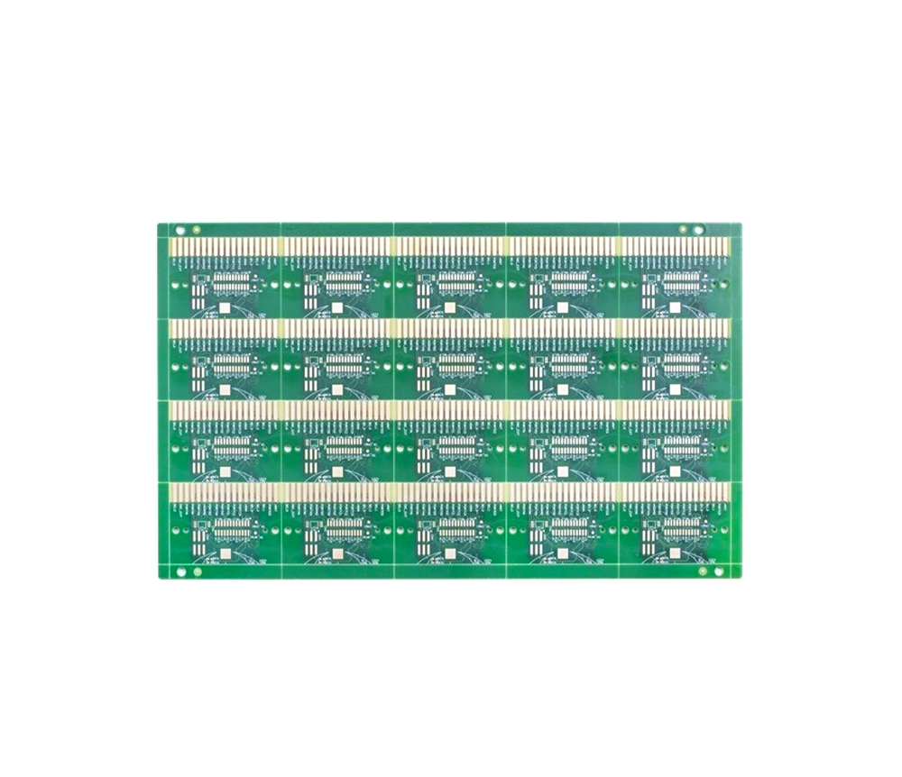
Copper clad panels were truly adopted on a large scale in PCB production, first appearing in the US PCB industry in 1947. The PCB substrate material industry has also entered its early stage of development. During this stage, the manufacturing technology progress of the raw materials used in the manufacturing of substrate materials - organic resins, reinforcing materials, copper foil, etc. - provides a strong driving force for the development of the substrate material industry. As a result, the manufacturing technology of substrate materials is gradually maturing. The invention and application of integrated circuits, as well as the miniaturization and high-performance of electronic products, have pushed PCB substrate material technology onto the track of high-performance development. The rapid expansion of demand for PCB products in the world market has led to rapid development in the production, variety, and technology of PCB substrate materials. At this stage, a broad new field

1. Drilling machine: used for drilling circuit boards. 2. Nailing machine: Fix or stack one or more double-sided boards with pipe position nails to facilitate positioning during drilling. 3. Grinding drill bit machine: The drill bit used for grinding and drilling. 4. Up and down rubber granulator; Fix the length of the rubber particles dropped from the drilling nozzle at 0.800 "± 0.005" for use by the drilling rig, or remove the rubber particles from the drilling nozzle. 5. Nail withdrawing machine; Use double-sided board drilling to retract pipe position nails. 6. Drilling machine: Used for drilling pipe position holes on the bottom plate.
Inquiry Now

