 +86 755 2794 4155
  sales@knownpcb.com
-
Shenzhen KNOWNPCB Technology Co., Ltd.
 +86 755 2794 4155
  sales@knownpcb.com
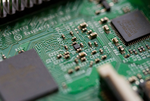
Have you noticed that now more and more of our lighting is using led lighting.What is LED? Compared to the traditional light bulbs, LEDs have lower power consumption, longer lifetime and higher energy efficiency. In the PCB industry,when we say LED PCB, it refers to the pcb used for LED lighting, if you are looking for a suitable LED PCB for your lighting system, this article may bring you something. WHAT ARE LEDS COMPOSED OF?LED is an initial light-emitting diode that produces light when an electric current passes through. LEDs typically have negative and positive electrodes, which generate light in the visible light region.The LEDS are glued to the PCB by soldering process and have electrical connections for lighting.Since light-emitting diodes dissipate a lot of heat when they are in use, when you are designing LED, the metal core is usually the best choice for LED PCB, it is because that it dissipates heat more faster. Among them, the metal material aluminum is the most widely used
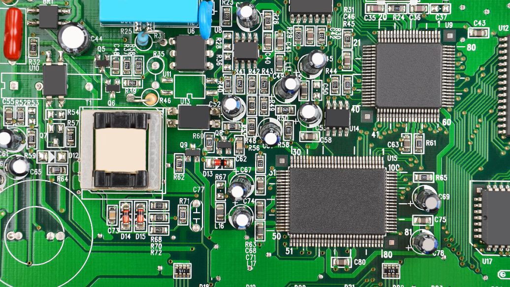
Sometimes, PCB circuit board substrates can cause open circuits, which are mainly caused by: 1. There are scratches on the copper clad plate before entering the warehouse; 2. The copper clad plate was scratched during the cutting process; 3. The copper clad plate was scratched by the drilling nozzle during drilling; 4. The copper clad plate was scratched during transportation; 5. The surface copper foil was damaged due to improper operation during the stacking of boards after copper deposition; 6. The copper foil on the surface of the production board was scratched when passing through the leveling machine. Improvement methods: 1. Before entering the warehouse, the IQC must conduct spot checks on the copper clad PCB circuit board substrate to check if there are scratches or exposed substrate on the board surface. If there are any, the supplier should be contacted in a timely manner to make appropriate treatment based on the actual situation. 2. The PCB circuit board substr
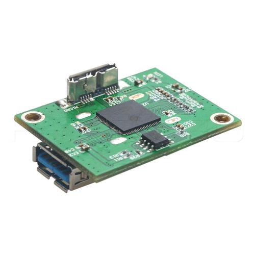
After decades of development, the PCB circuit board industry has become extremely mature in terms of technology. Key technologies such as drilling, copper deposition, exposure, development, and etching have been well controlled by automation equipment, making PCB circuit board factories an equipment and fixed asset intensive industry. Business owners have to come up with low price strategies in the fierce market competition. Therefore, the market will be full of the phenomenon of Gresham's law. How to stand out from fierce market competition? It is worth every manager's deep thinking.The rise of any industry is first about creativity, then about the market, and finally about quality. At the beginning, insightful individuals will first identify potential market opportunities, enter the market first, and quickly gain profits. Then more and more people will discover such business opportunities and enter the market competition. Finally, when the industry is saturated, end customers can fre
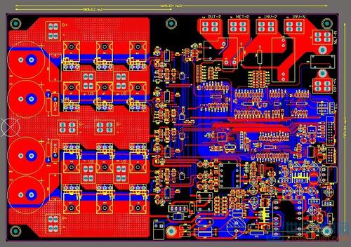
The competition of enterprises is diversified, from the previous short Plate theory theory to the current long Plate theory theory. Faced with fierce market competition, limited resources of enterprises can only be concentrated on a certain board, making it bigger and stronger. This has led many electronic product companies to only focus on research and development and sales, outsourcing PCBA electronic manufacturing to professional companies, and no longer trying out material procurement, outsourcing processing, supply chain management, and so on that they are not good at. The benefit of doing so is to reduce manpower investment and management costs, as well as the risk losses caused by one's lack of expertise. Careful people will find that in recent years, more and more companies have begun to seek professional PCBA electronic manufacturing resources.Another driving factor is the country's advocacy for mass entrepreneurship and innovation, which has led to an increasing number of sma
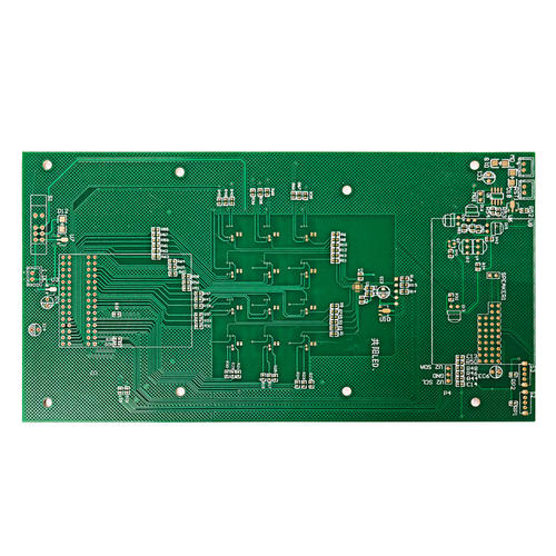
(1) Although the wiring spacing and wiring width are consistent, the spacing of Coupon Test point is fixed at 2.54mm (to meet the spacing of test probes), and the spacing of the end of the actual wiring in the board (i.e., the golden finger) is variable. With the emergence of QFP, PLCC, and BGA packages, the pin spacing of some chips is far less than 2.54mm (i.e., the spacing of Coupon Test point).(2) Coupon wiring is an ideal straight line, while the actual wiring on the board is often designed and produced according to actual needs. PCB designers and production personnel can easily idealize Coupon's wiring, but the actual wiring on the PCB board may undergo irregular changes due to practical needs.(3) The positions of Coupon and the actual wiring inside the board are different on the entire PCB board. Coupons are located in the middle or edge of the PCB board and are often removed by the manufacturer when the PCB board leaves the factory. The actual positions of the wiring inside the
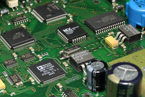
(1) The distance between the Test point of Coupon is different from that of the cabling of Coupon, which will cause impedance discontinuity between the Test point and the cabling. This will result in different impedance test results.(2) The impedance changes reflected by curved wiring and ideal wiring are inconsistent. The characteristic impedance at the bending and turning point of the wiring is often discontinuous, while Coupon's idealized wiring cannot reflect the impedance discontinuity caused by the bending of the wiring.(3) Coupon and real wiring have different positions on the PCB board. Currently, PCB boards are designed with multi-layer wiring and require pressing during production. When a PCB board is pressed, the pressure on different positions of the board cannot be consistent, and the thickness of the dielectric layer at different positions will also vary. As a result, the dielectric constant of the PCB board made from this method often varies at different positions, and t

(1) Visual inspection PCB boards generally undergo electrical testing before leaving the factory. We inspect the appearance of PCB boards through visual inspection methods upon receipt, including warping, scratches, flying wires, broken wires, ink blockage, unclear screen printing, solder pad oxidation, uneven solder pads, blocked vias, and burrs on the board edges (2) Dimensional measurement Use a micrometer to measure the thickness, shape, dimensions, and V-CUT of the PCB board to ensure compliance with the Gerber file design. (3) Furnace temperature test Many PCB boards, due to poor process control, experience yellowing and warping when subjected to high temperatures such as reflow soldering. When outsourcing processing, it is essential to require the PCB board to undergo furnace temperature testing first to avoid mass welding defects or affecting the future reliability and durability of the product. Especially for PCB boards with high TG design, this inspection is particular
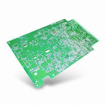
After the electronic product development project is finalized, engineers and procurement departments need to estimate the price of the entire PCBA circuit board. The simple method is to send the design BOM and GERBER files to different suppliers to obtain quotations for comparison. But the problem is that when there is a significant difference in the price of PCBA we obtain, we cannot determine the true and accurate price. Because different suppliers may substitute materials or make random estimates, which can mislead your prices. At this time, it is particularly important to self estimate the price of PCBA processing. PCBA processing price mainly includes: component cost, PCB cost, SMD processing cost, and basic Gross profit of manufacturing enterprises. The cost of components can be inquired through the public Open platform (Tradegate, Datagate), and its open price can be used as a reference. For large goods above 10K, it can generally be estimated at 70% of the open price. The

The steel mesh tension standard has reference indicators in the IPC electronic acceptance standard. Generally, a steel mesh tension tester is used, placed at a distance of 15-20cm from the edge, and 5-8 points are selected, with each square centimeter having a tension greater than 35-50N. Every time the steel mesh is used online, the tension must be re measured. The testing steps are as follows: Appearance inspection of steel mesh: whether there are scratches, burrs, damages, etc Zero the tension gauge and tighten the zero scale screw The steel mesh should be placed horizontally on the workbench and should not be pressed by hand during testing Select a Test point to check whether the test value meets the standard Fill out the "Steel Mesh Tension Test Record Form" Steel mesh cleaning Installation and use on solder paste printing machine

1. Does the voltage and current meet the design requirements Under normal circumstances, after each PCBA is powered on, even without burning the MCU program, various voltage differences, current conduction, etc. can be generated through circuit connections. PCB designers will deploy different Test point on the PCBA board, and these Test point can be connected to the ICT or FCT test rack to detect voltage and current data. 2. After burning MCU program, input user actions and check whether the output is normal After the PCBA board burns the MCU program, the user executes an action (such as long pressing the switch for 3 seconds), and the MCU will issue a logic command to control the circuit's switch, thereby achieving the design requirements. In this case, PCBA online test can detect whether the input and output of this action are normal. 3. Full functional testing at the product level This online testing is relatively advanced, basically simulating more than 80% of the core fun
Engineering and technical personnel should understand the necessary production processes and master relevant software production, including common circuit design software such as Altium Designer, Pads2000, Autocad, etc. They should also be familiar with necessary CAM software such as View2001 and CAM350; GCCAM, etc., should include PCB design input, which can edit, correct, repair, and assemble circuit graphics, use magnetic disks as the dielectric material, and output automated data for photo drawing, drilling, and testing. An important aspect of the success of the laser light drawing machine market is providing manufacturers with a large amount of technical strength in engineering production. At the same time, we have also seen a large demand for engineering and production personnel from Jianhe PCB manufacturers, as well as an increasing demand for the level of engineering and technical personnel. Therefore, it prompts us to continuously improve our technical level in order to m

The level of PCB engineering production can reflect the design level of designers, as well as the production process and technical level of printed board manufacturers. At the same time, as the PCB engineering production integrates Computer-aided design and auxiliary manufacturing, it requires extremely high precision and accuracy, otherwise it will affect the electrical performance of the final electronic products on board, and may cause errors in serious cases, which will lead to the scrapping of the whole batch of printed board products, delay the manufacturer's contract delivery time, and suffer economic losses. Therefore, as a PCB engineering manufacturer, one must always bear in mind their significant responsibilities and not take them lightly. They must be careful, serious, and meticulous. When processing PCB design files, it is important to carefully check whether the received files comply with the rules established by the designer? Can it meet the requirements of PCB manuf

The circuit board has a history of over 60 years since its invention. History has shown that without circuit boards and electronic circuits, flight, transportation, atomic energy, computers, aerospace, communication, home appliances... all of these cannot be achieved. The truth is easy to understand. Chips, ICs, and integrated circuits are the grain of the electronic information industry. Semiconductor technology reflects a country's level of industrial modernization and guides the development of the electronic information industry. The electrical interconnection and assembly of semiconductors (integrated circuits, ICs) must rely on circuit boards. As the author of Japan's "Circuit Board Collection", Masao Kobayashi, said, "Without computers and data, electronic devices are like an ordinary box; without semiconductors and circuit boards, electronic components are like ordinary stones." PCB is a promising industry in China, with double-digit growth rates every year. Many foreign ord
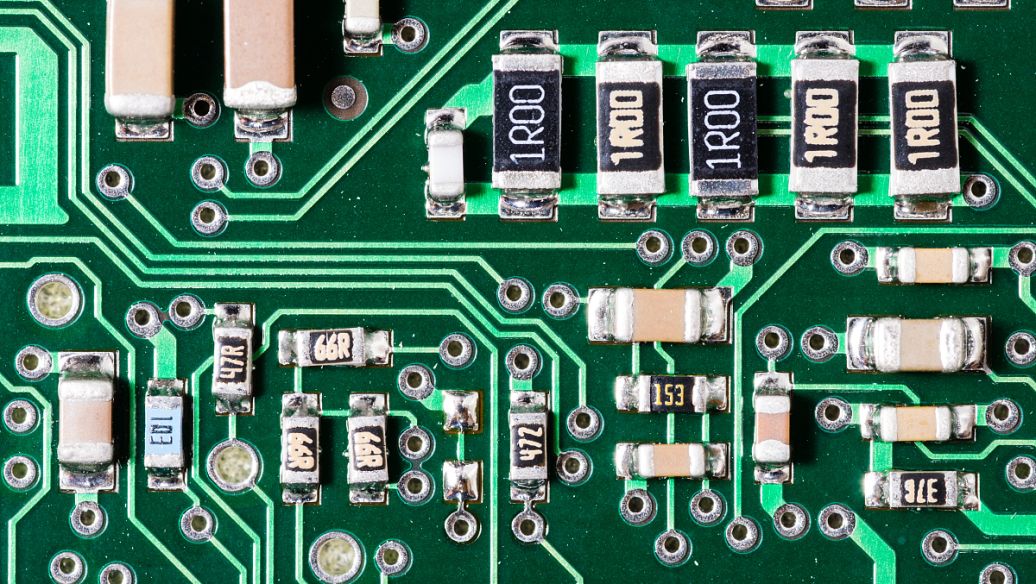
Circuit board maintenance is an emerging repair industry. The automation level of industrial equipment is increasing, so the number of industrial control boards in various industries is also increasing. After the industrial control boards are damaged, the high cost of replacing circuit boards (ranging from several thousand yuan to tens of thousands or hundreds of thousands of yuan) has become a very headache for enterprises. In fact, the vast majority of these damaged circuit boards can be repaired in China, and the cost is only 20-30% of purchasing a new board, which takes much shorter time than ordering a board abroad. Below is an introduction to the basic knowledge of circuit board maintenance. Almost all circuit board maintenance has no drawings and materials, so many people are skeptical of circuit board maintenance. Although various circuit boards are different, what remains unchanged is that each circuit board is composed of various integrated blocks, resistors, capacitors a
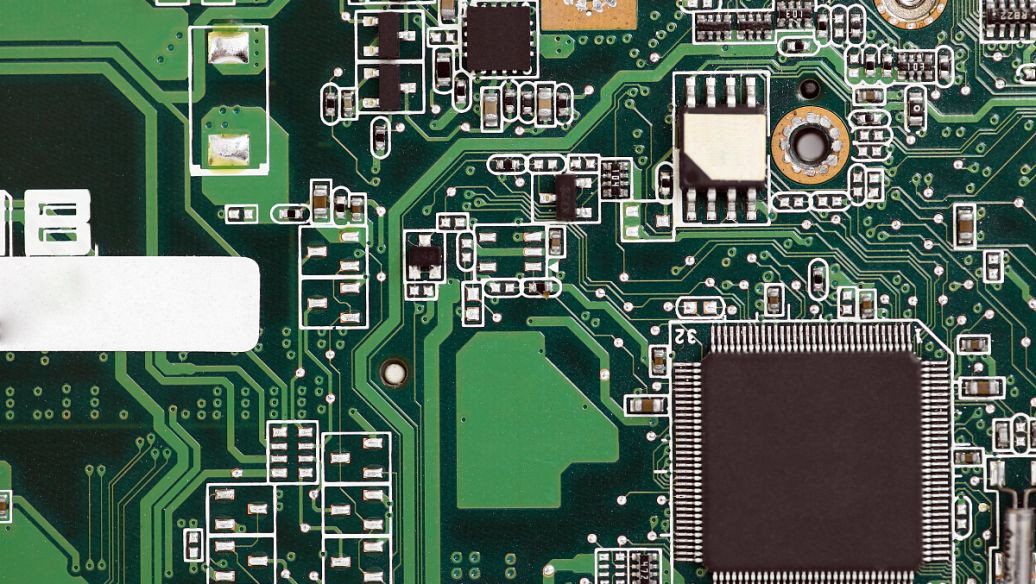
PCB connector This bottom contact connector has specifications of 4 to 8 circuits, with a rated current and voltage of 0.3A and 50V, and can be used for 0.12mm thick FPC cables. It has a unique BackFlip clamp that facilitates the insertion and extraction of cables in tight spaces, as well as strong FPC cable clamping force. The PCB connector industry in Chinese Mainland is one of the few regions not affected by the global economic recession. As the domestic and international market demand is strong, with the development of electronic equipment to higher transmission speed and smaller size, connectors also follow this trend. Therefore, chip connectors, optical fiber connectors Connector products such as wired broadband connectors and micro spacing connectors suitable for various portable/wireless electronic devices are expected to become future star products.

PCB series connectors: used in military aviation, railway projects, industrial projects, aerospace projects, testing instrument ship systems, electric sightseeing vehicles; UPS; Communication power supply; The preferred high current connector for products such as chargers and batteries. The connector is made of PBT material, which has excellent electronic and motor characteristics and can be widely used in industrial needs. Various electric vehicles, including electric buses, forklifts, golf carts, sightseeing vehicles, tractors, batteries, communication power supplies; UPS. AC/DC stabilized power supply. EPS. inverter, high-frequency module power supply and high-frequency charger system, electric machinery; Electric wheelchairs, electric floor scrubbers, lawn mowers, vacuum cleaners, medical equipment; Suction machines, pressure reducing machines, electric treatment beds; Power supply, Material-handling equipment, rechargeable battery application, power distribution equipment, indu

The insulation is made of German Bayer flame-retardant polycarbonate raw materials, ensuring your safe use. The plastic base shall prevent unqualified phenomena such as extrusion deformation and long-term fracture. After secondary manual inspection of the screws and nuts, there will be no signs of screw jamming, slipping, and difficulty in disassembly. The terminal connection piece is free of burrs, patterns, secure clamping, good coating, excellent conductivity, and good verticality of the connection piece. This product adopts a wire spring contact pair, and the socket automatically shortens when the plug and socket are separated by 4mm. This product has high reliable electrical contact performance, novel structure, convenient use, small size, soft insertion and extraction, long service life, low contact resistance, good insulation performance, anti-interference, and other characteristics. Widely applicable to electrical control equipment in power system relay protection control

Its working principle is: usually, a conductive pattern made of printed circuits, printed components, or a combination of both on insulating materials according to predetermined design is called a printed circuit. The conductive pattern that provides electrical connections between components on an insulating substrate is called a printed circuit. In this way, printed circuits or finished boards of printed circuits are called printed circuit boards, also known as printed boards or printed circuit boards. The gold soldering area on the PCB lowers the PCB board edge In industrial environments, connectors produced using press fit technology can maintain stability and can be used with right angle PCBs This nano compact connector is suitable for various drones, especially in extremely harsh working environments The advantage of using this connector in drone applications is that the oversupply of basic PCB connectors with small size has forced their prices to decrease by 3% to 10%. Manuf
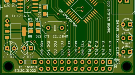
The product meets the 19 "standard and adopts a splicing method of profiles and plates, which is easy to assemble and fully reflects the characteristics and advantages of standardization, modularization, and serialization. The product adopts a modular card structure with good scalability, which can be expanded according to customer needs and is easy to maintain in the later stage. Has good electromagnetic shielding performance. For special functional requirements such as EMC (electromagnetic shielding and anti-interference) and ESD (live plug and unplug maintenance), both design and functionality have passed product testing certification. It has reliable anti strength vibration design, impact design, and load-bearing design (superior performance in rail transit). Excellent heat dissipation performance and environmental protection design (IP protection level). Effective lightweight design: The product is made of aluminum alloy material, which is lightweight and effective, and has
Circuit board moisture-proof insulation coating adhesive is specifically designed for PCB circuit boards and various plastic surfaces to provide protection after coating. The surface of the covered material has functions such as moisture resistance, insulation, dust prevention, and corona prevention. Typical applications include PCB circuit boards, solar panels, bathroom sensors, ink, paper drawings, and more 1. There are a wide range of bonding materials, suitable for various circuit board substrates, plastics, glass, and metals. Oil coated paper and other materials have extremely high adhesion 2. The surface of the adhesive solidifies (surface drying) quickly, and can quickly reach surface drying under ultraviolet light irradiation. 3. It can cover the surface of PCBs, soft plastics, and oil coated paper paintings 4. Low viscosity and permeability, which can be sprayed mechanically 5. It is moisture-resistant, high-temperature resistant, high humidity resistant, and UV resis
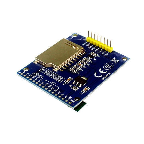
1. The ideal adhesive layer thickness for bonding is 0.01-0.05mm, and either too thin or too thick can affect the bonding performance. 2. Ensure that the adhesive layer absorbs sufficient ultraviolet energy to achieve the best curing effect, otherwise it may affect the adhesive performance of the adhesive layer. 3. Do not move the material back and forth when exposed to ultraviolet radiation, otherwise it may cause the adhesive layer to turn white and the bonding strength to decrease. 4. The remaining glue should not be returned to the original packaging, and should be stored at room temperature and sealed away from light, avoiding contact with children. 5. This product has slight irritation to the eyes and skin. If it accidentally splashes into your eyes, please rinse immediately with plenty of water. If in contact with skin, Rinse with soap. If the situation is serious, please see a doctor. It is recommended that the glue applicator wear professional UV resistant glasses and
Inquiry Now

