 +86 755 2794 4155
  sales@knownpcb.com
-
Shenzhen KNOWNPCB Technology Co., Ltd.
 +86 755 2794 4155
  sales@knownpcb.com
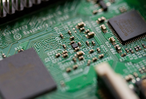
Have you noticed that now more and more of our lighting is using led lighting.What is LED? Compared to the traditional light bulbs, LEDs have lower power consumption, longer lifetime and higher energy efficiency. In the PCB industry,when we say LED PCB, it refers to the pcb used for LED lighting, if you are looking for a suitable LED PCB for your lighting system, this article may bring you something. WHAT ARE LEDS COMPOSED OF?LED is an initial light-emitting diode that produces light when an electric current passes through. LEDs typically have negative and positive electrodes, which generate light in the visible light region.The LEDS are glued to the PCB by soldering process and have electrical connections for lighting.Since light-emitting diodes dissipate a lot of heat when they are in use, when you are designing LED, the metal core is usually the best choice for LED PCB, it is because that it dissipates heat more faster. Among them, the metal material aluminum is the most widely used

1.1. When the cutting machine is turned on, do not reach into the machine. 2.2. Flammable materials such as paper should not be placed next to the oven to prevent fires. 3.3. The temperature setting of the oven must not exceed the specified value. 4.4. Asbestos gloves must be worn when removing boards from the oven, and the boards must be removed after they have cooled down. 5.5. Dispose of waste materials strictly according to the method specified in MEI001 to prevent environmental pollution. Cutting board 1. Equipment: manual plate cutting machine, target milling machine, CCD Hole punch, gong machine, edging machine, word marking machine, thickness gauge; 2. Function: Laminate shape processing, preliminary forming; Process: Dismantling board → Dotting and drawing lines → Cutting large board → Milling copper skin → Punching → Forming gong edge → Grinding edge → Typing mark → measuring plate thickness

1、 Purpose: Cut large pieces of sheet metal into small pieces of various required specifications. 2、 Process flow: 3、 Equipment and function: 1. Automatic cutting machine: Cut large materials into various fine materials. 2. Rounding machine: Grind the dust ends of the plate corners to a round shape. 3. Washing machine: Clean and air dry the dust and impurities on the board machine. 4. Oven: Furnace board to improve the stability of the board material. 5. Word marking machine; Type a label on the edge of the board for marking. 4、 Operating specifications: 1. Before starting the automatic feeding machine, check the set size to prevent incorrect feeding. 2. After cutting the inner layer board, attention should be paid to adding marks to separate the materials horizontally and vertically, and avoid confusion. 3. When handling the board, gloves should be worn and handled with care to prevent scratching the board surface. 4. After washing the board, it is necessary to pay at
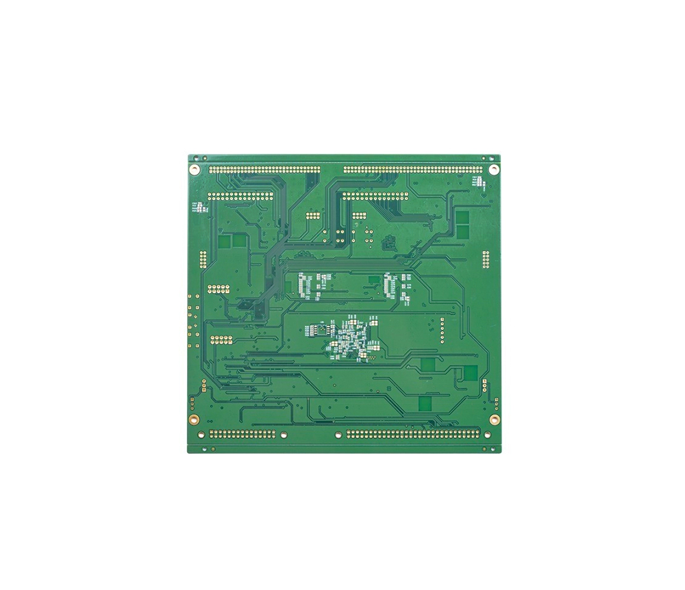
The drill types of PCB drill bit control drilling machine: the drill bits for PCB drilling include straight shank Fried Dough Twists drill, fixed shank Fried Dough Twists drill and fixed shank shovel drill. Straight handle Fried Dough Twists drills are mostly used for single head drilling machines to drill simple printed boards or single panels. Now they are rarely seen in large printed board manufacturers, and their drilling depth can reach 10 times the drill diameter. When the substrate layer is not high, using a drill sleeve can avoid drilling deviation. At present, most manufacturers use CNC drilling machines, which use fixed shank drill bits made of hard alloy and can achieve automatic replacement of drill bits. High positioning accuracy, no need to use drill sleeves. Large helix angle, fast chip removal speed, suitable for high-speed cutting. Within the full length range of the chip removal groove, the diameter of the drill bit is an inverted cone, resulting in less friction
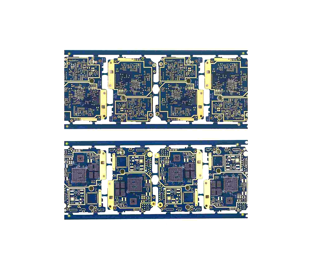
1. The ideal adhesive layer thickness for bonding is 0.01-0.05mm, and either too thin or too thick can affect the bonding performance. 2. Ensure that the adhesive layer absorbs sufficient ultraviolet energy to achieve the best curing effect, otherwise it may affect the adhesive performance of the adhesive layer. 3. Do not move the material back and forth when exposed to ultraviolet radiation, otherwise it may cause the adhesive layer to turn white and the bonding strength to decrease. 4. The remaining glue should not be returned to the original packaging, and should be stored at room temperature and sealed away from light, avoiding contact with children. 5. This product has slight irritation to the eyes and skin. If it accidentally splashes into your eyes, please rinse immediately with plenty of water. If in contact with skin, Rinse with soap. If the situation is serious, please see a doctor. It is recommended that the glue applicator wear professional UV resistant glasses and

① The 1000 series represents the 1050, 1060, and 10701000 series aluminum plates, also known as pure aluminum plates. Among all the series, the 1000 series has the highest aluminum content, with a purity of over 99.00%. Due to the absence of other technical elements, the production process is relatively simple and the price is relatively cheap, making it the most commonly used series in conventional industries. The majority of the products circulating in the market are the 1050 and 1060 series. The minimum aluminum content of the 1000 series aluminum plate is determined based on the last two digits. For example, the last two digits of the 1050 series are 50. According to international brand naming principles, the aluminum content must reach 99.5% or above as a qualified product. In China's aluminum alloy technical standard (GB/T3880-2006), it is also explicitly stipulated that the aluminum content of 1050 should reach 99.5%. The same principle applies to 1060 series aluminum plates

Audio devices Input and output amplifiers, balanced amplifiers, audio amplifiers, preamplifiers, power amplifiers, etc. Power supply equipment Switch regulator, DC/AC converter, SW regulator, etc. Communication electronic equipment High frequency amplifier, filtering device, and reporting circuit. Office automation equipment Motor drivers, etc. automobile Electronic regulators, igniters, power controllers, etc. computer CPU board, floppy drive, power device, etc. Power module Inverter, solid-state relay, rectifier bridge, etc. Lamps Lighting With the promotion of energy-saving lights, various energy-saving and colorful LED lights have become popular in the market, and aluminum substrates used for LED lights have also begun to be widely used
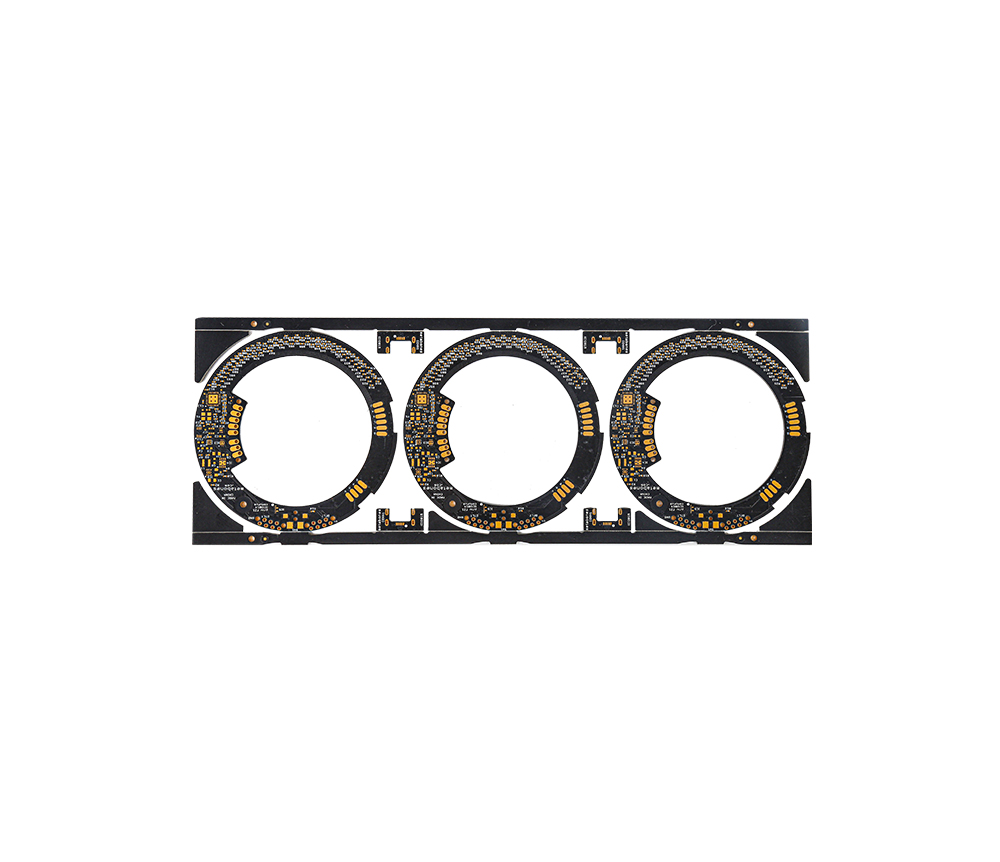
Material: Plastic; It can effectively release the static charges accumulated on the surface of the object, so that it does not generate charge accumulation and high potential difference; It has multiple advantages such as toughness, wear resistance, moisture and corrosion prevention, thermal insulation and shock resistance, economy and durability. The anti-static turnover rack can greatly reduce the damage rate of electronic products during the production process, reduce costs, and improve product quality and profits; The main purpose of the anti-static turnover rack is to eliminate static electricity, and it is widely used for the turnover loading and storage of PCB boards during the production process. Resistance value: below the 6th power of 10; L-shaped turnover rack, also known as PCB board turnover rack, is widely used in SMT processing, machinery, automobiles, home appliances, light industry, electronics and other production enterprises. It is acid and alkali resistant, oil
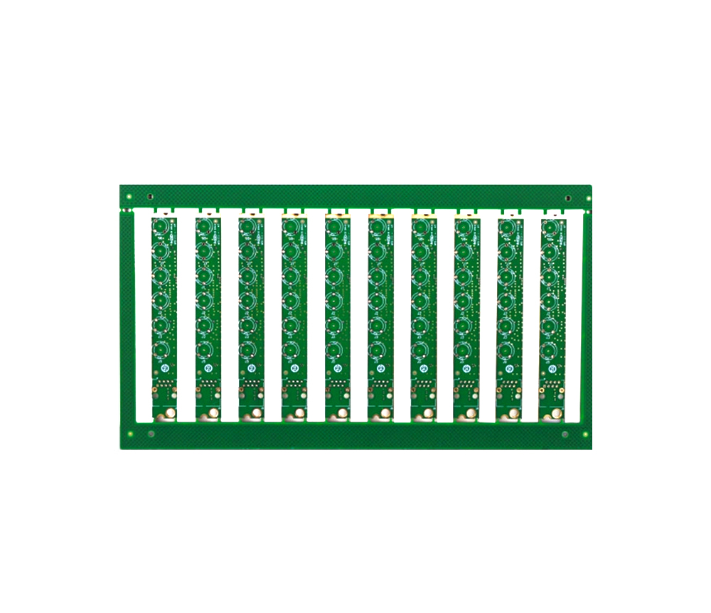
PCB double -sided rigid printed board Double -sided rigid version → double -sided copper covered plate → feeding → stack board → CNC diamond guide pores → test, removing burr brush → chemical plating (metal of guide holes) → (full board electroplating thin copper) → inspection brush → Net Printing circuit graphics, curing (dry membrane or wet film, exposure, development) → inspection, repair board → line graphics electroplating → electroplating (anti -nickel/gold) → de -printed (sensor) → etching copper → (( Retirement) → Clean brush → Net printing and welding graphics commonly used thermal solidification green oil (light -sensitive dry film or wet film, exposure, development, thermal solidification, commonly used sensor thermal solid green oil) → cleaning, drying → net print marking character graphics graphics graphics graphics graphics graphics graphics graphics , CITC → (spray tin or organic welding film) → Machining → cleaning, drying → electrical interrupt detection → inspectio
PCB process flow chart It can be seen from the process flowchart that the multi -layer board process is developed on the basis of double -faced metal chemical technology. In addition to the two -sided process, it also has several unique contents: the inner layers of metalized holes, drilling and removing epoxy drilling, positioning system, layer pressure, and special materials. Our common computer board card is basically a two -sided printed lineboard of epoxy resin glass, one of which is the other side of the installation element and the other side of the component foot welding surface. The component foot divide vertical welding surface we call it as a pad. Why don't other copper -guided line figures not on tin? In addition to the pads and other parts of tin welding, the other parts have a layer of welded welding film. Most of its surface welded films are green, and a few use yellow, black, blue, etc. Therefore, in the PCB industry, welding oil is often called green oil. Its role
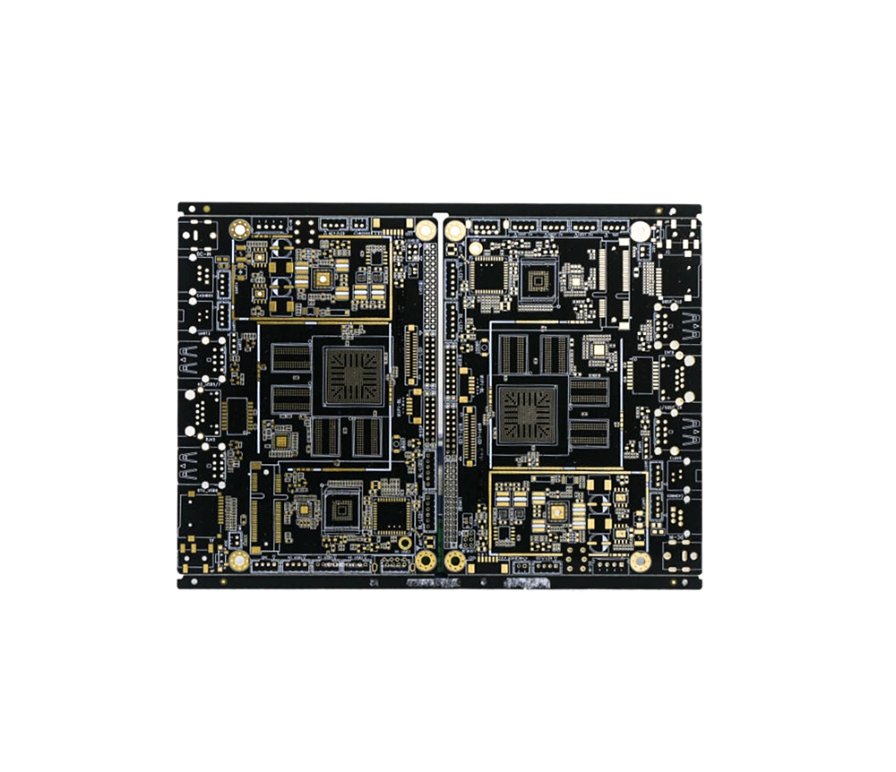
PCB surface installation 1) Because the printed board has eliminated a large number of large -guided pores or buried holes interconnect technology, the wiring density on the printing board is increased, and the area of the printed board is reduced (generally one of the three -pointers for inserted installation), and at the same time It can also reduce the number of design layers and costs of the printed board. 2) Reduce weight and improve seismic performance, and adopts glue welded and new welding technology to improve product quality and reliability. 3) Due to the increased wiring density and shortening the length of the lead, the parasitic capacitance and parasitic inductance are reduced, which is more conducive to increasing the electrical parameter of the printed board. 4) It is easier to automate more than the installation installation, improves the installation speed and labor productivity, and reduces the assembly cost accordingly. From the above surface safety technology
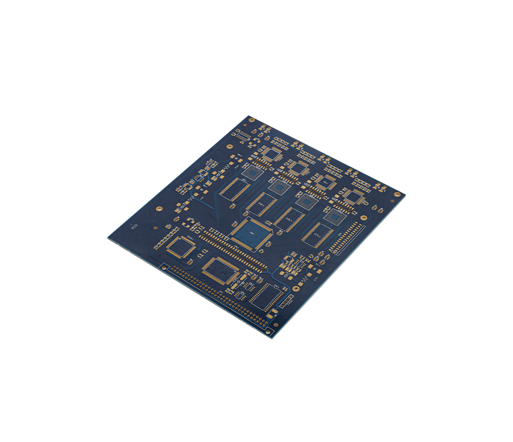
PCB printing 1. Live board printing There are many texts, few photos and pictures, there are many opportunities for changes in text, and the number of prints is not large -printed products between hundreds or thousands of printeds should be printed in live version. The number of divery printing should not exceed 30,000, and the fine picture electric version should not exceed 70,000 to 80,000. The printing pictures must be used to obtain a perfect outlet. Therefore, you cannot use cheap paper to print pictures and want to achieve exquisite results. When using the live version of the duct, the line of the line is easy to separate and disconnect, which is a common disadvantage. In addition, when the printing pressure is too large or the surface layer of the pressure cylinder is too soft, it will make the back of the finished product printing with relief, which will greatly reduce the quality of the print. 2. Silk net printing Because the screen printing and printing ink are particul
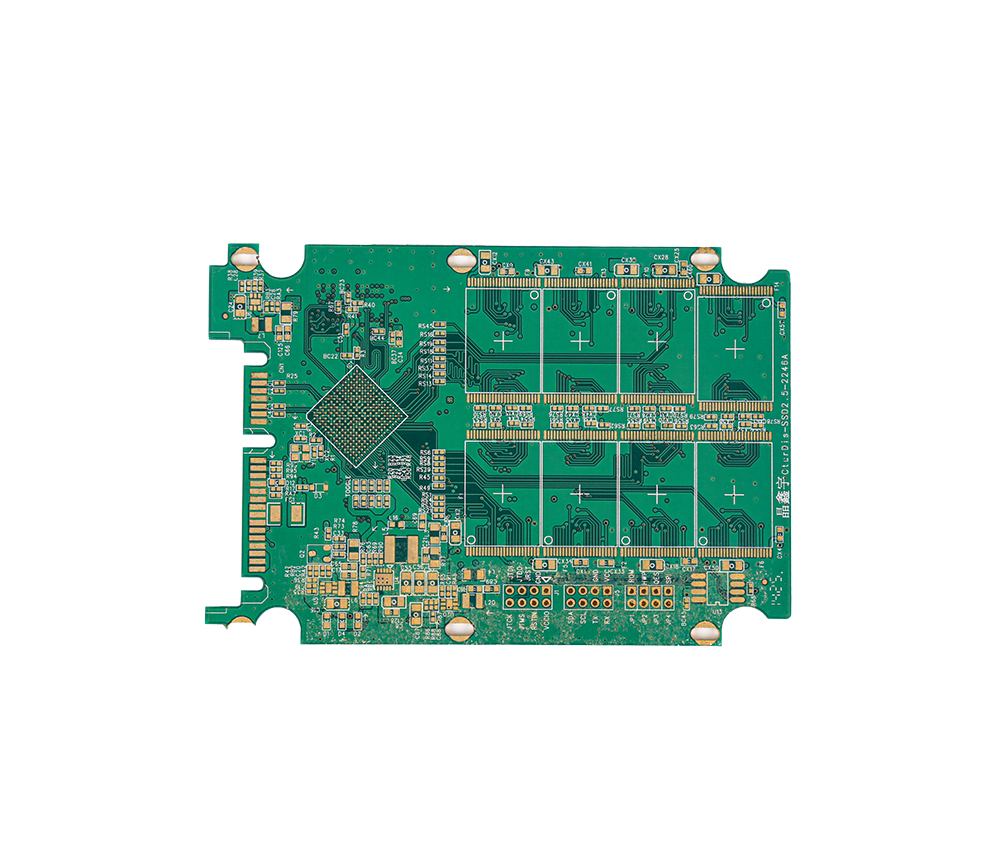
PCB generally includes 1. Program ID (PID, process handle): It is unique, and each process must correspond to a PID. PID is usually an integer number 2. Feature information: general subsystem processes, user processes, or kernel processes, etc 3. Process status: running, ready, blocked, indicating the current running status of the process 4. Priority: Indicates the priority size for obtaining CPU control 5. Communication information: a reflection of the communication relationship between processes, as the operating system provides communication channels 6. On site protection zone: used to protect blocked processes 7. Resource requirements and allocation control information 8. Process entity information, indicating the program path and name, whether the process data is in physical memory or in swap partitions (pagination) 9. Other information: work unit, workspace, file information, etc
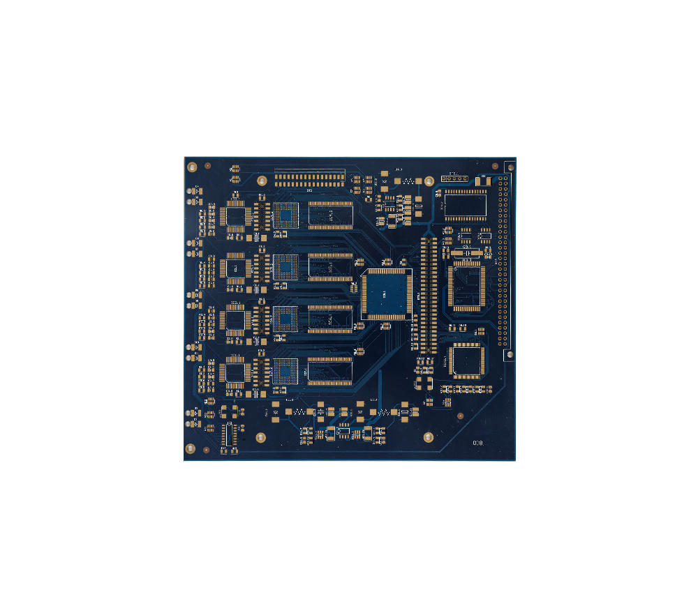
PCB polychlorinated biphenyls Polychlorinated biphenyls were artificially synthesized organic compounds used commercially in North America from 1929 to the late 1970s. Although Canada did not process and produce this chemical substance, it has been widely used in electrical equipment insulation, heat exchangers, water systems, and other special applications. It took decades for people to realize the global environmental pollution caused by polychlorinated biphenyls, which are mixtures of various chlorinated biphenyls and pose great harm to human health. The Canadian government once took measures to try to eliminate PCBs, but in 1977, illegal imports, processing and sales of PCBs occurred in Canada, and in 1985, PCBs were illegally released to the natural environment. The Canadian Constitution allows PCB equipment owners to continue to use PCBs until the life of the equipment. Since 1988, provincial governments in Canada have only begun to regulate the storage, transportation, and d
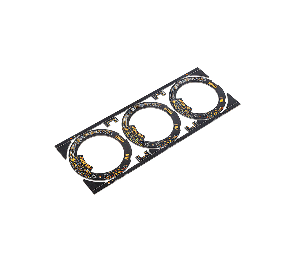
PCB plug terminal Part of the wire is pressed tightly and then inserted into another part, which is welded to the PCB board. The bottom mechanical principle of this connection ensures the long-term airtight connection of the product and the reliability of the finished product through this anti vibration design. Both ends of the socket can be equipped with mounting ears, which can greatly protect the connectors and prevent poor placement of the connectors. At the same time, this socket design ensures that the socket can be correctly inserted into the mother body. Sockets can also have assembly and locking buckles. The assembly buckle can be more firmly fixed to the PCB board, and the locking buckle can lock the mother body and socket after installation is completed. 1. Curved and straight pin plug terminals (incoming direction at 270, 180, and 90 degrees to PCB board) 2. Fixed with screw flange ears and flange without screws 3. Screw connection and spring connection 4. Spacing: 3
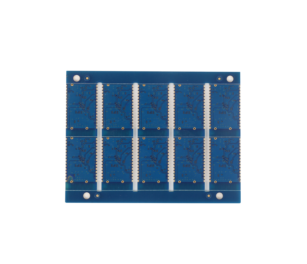
PCB insertion and extraction force detection The reason for the inspection is that there are burrs or dirt stuck at the screw teeth of a few installation holes. Especially when using the last few installation holes that have already been connected to a plug-in terminal plug socket by the factory, if the defect is found, the crimping wires of the other holes that have already been installed must be removed one by one and the plug socket replaced. In addition, due to improper matching of wire diameter and crimping aperture, or due to incorrect crimping process operation, it can also cause accidents of unstable crimping ends. For this reason, the production factory needs to conduct a test on all installation holes of the delivered plug (socket) samples before the finished product leaves the factory, that is, use loading and unloading tools to simulate the wires with crimped pins or sockets and send them in place to check whether they can be locked. According to the product technical sp
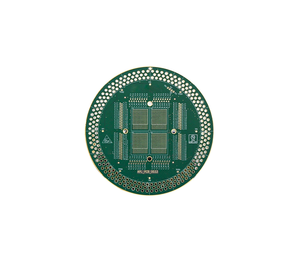
PCB self-service selection NC, is the internal product number of Nachuan Electric 1.5 refers to the cross-sectional area of the product being 1.5mm 2. Refers to the number of terminal positions, and the number of digits can be changed as a parameter ST, referring to the plug 3.50, which refers to a variable parameter with a spacing of 3.50 If: NC 1.5/2-STF-3.50 plug-in terminal blocks, only ST becomes STF, indicating a flange with side screws The terminal housing is usually labeled with product information, which allows users to identify the basic parameters of the product to prevent operational errors during installation and connection, and can play a simple preventive role. There are permanent markings on the main parts of the shell as follows: a. Terminal rated voltage (V) b. Terminal rated current (A) c. Terminal model d. Terminal trademark or manufacturer name e. Product Certification System
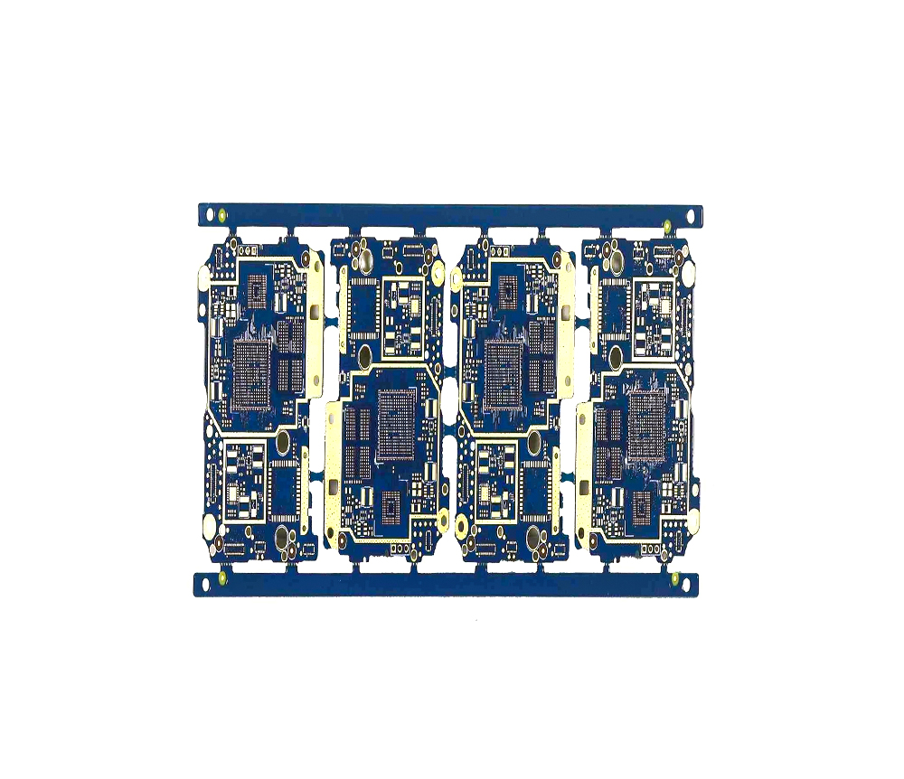
PCB gong board machine *Desktop single table cutting machine, with a speed of up to 100mm/s and a positioning speed of 500mm/s. *Capable of continuous cutting without interruption during loading and unloading. *A high-quality shaft system enables the system to quickly accelerate and decelerate, reduce synchronization time, improve productivity, and maintain high accuracy. *Use high-quality hardware to ensure high rigidity and performance. *All guide screws are covered to prevent dust and dirt from entering, thereby improving the lifespan and performance of the shaft. 1. Drive system motor: servo/stepper motor 2. Spindle speed: 50000r/s 3. Cutting performance: 500mm/s 4. Repetitive accuracy of driving system: ± 0.02mm 5. Cutting speed: Maximum 100mm/S depends on circuit board material and cutting quality 6. Resolution: ± 0.01mm 7. Configuration: X, Y, Z three axes, stroke: 300X300X80mm, stroke can also be customized. 8. Repetitive accuracy:<0.1mm, for the contours of stra
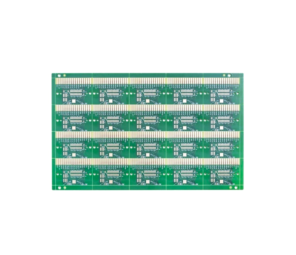
PCB upper shelf PCB loading rack, also known as PCB collection box, PCB automatic loading rack, SMT loading and unloading rack, etc. Widely applicable to automatic loading and unloading machines, it is acid resistant, oil resistant, high temperature resistant, non-toxic, and odorless. It can be used to hold PCB boards, making cleaning convenient, circuit board turnover convenient, stacking neatly, and easy to manage. Its reasonable design and excellent quality are suitable for transportation, distribution, storage, circulation and processing in factories. The SMT loading and unloading rack can be combined with various logistics containers and workstations, and is used in various warehouses, production sites, and other occasions. In today's world where automatic loading and unloading machines are increasingly valued by enterprises, the SMT loading and unloading rack helps complete the circulation, storage, and integrated management of PCB boards. It is a necessary product for modern

PCB upper shelf according to size 1. External dimensions: 355 * 315 * 580mm, can store 50 PCB boards. PCB board specifications: 350 * (80-250) mm PCB upper shelf Side plate guide groove. The groove depth is 3.5mm, the groove width is 8mm, and the pitch is 10mm 2. External dimensions: 355 * 320 * 563mm. Can store 50 PCB boards. PCB board specifications: 350 * (50-250) mm Side plate guide groove. The groove depth is 3.5mm, the groove width is 5mm, and the pitch is 10mm 3. External dimensions: 460 * 400 * 563mm. Can store 50 PCB boards. PCB board specifications: 460 * (100-330) mm Side plate guide groove. Groove depth 3.5mm, groove width 5mm, pitch 10mm 4. External dimensions: 535 * 460 * 570mm, can store 50 PCB boards. PCB board specifications: 535 * (50-390) mm Side plate guide groove. The groove depth is 3.5mm, the groove width is 5mm, and the pitch is 10mm.
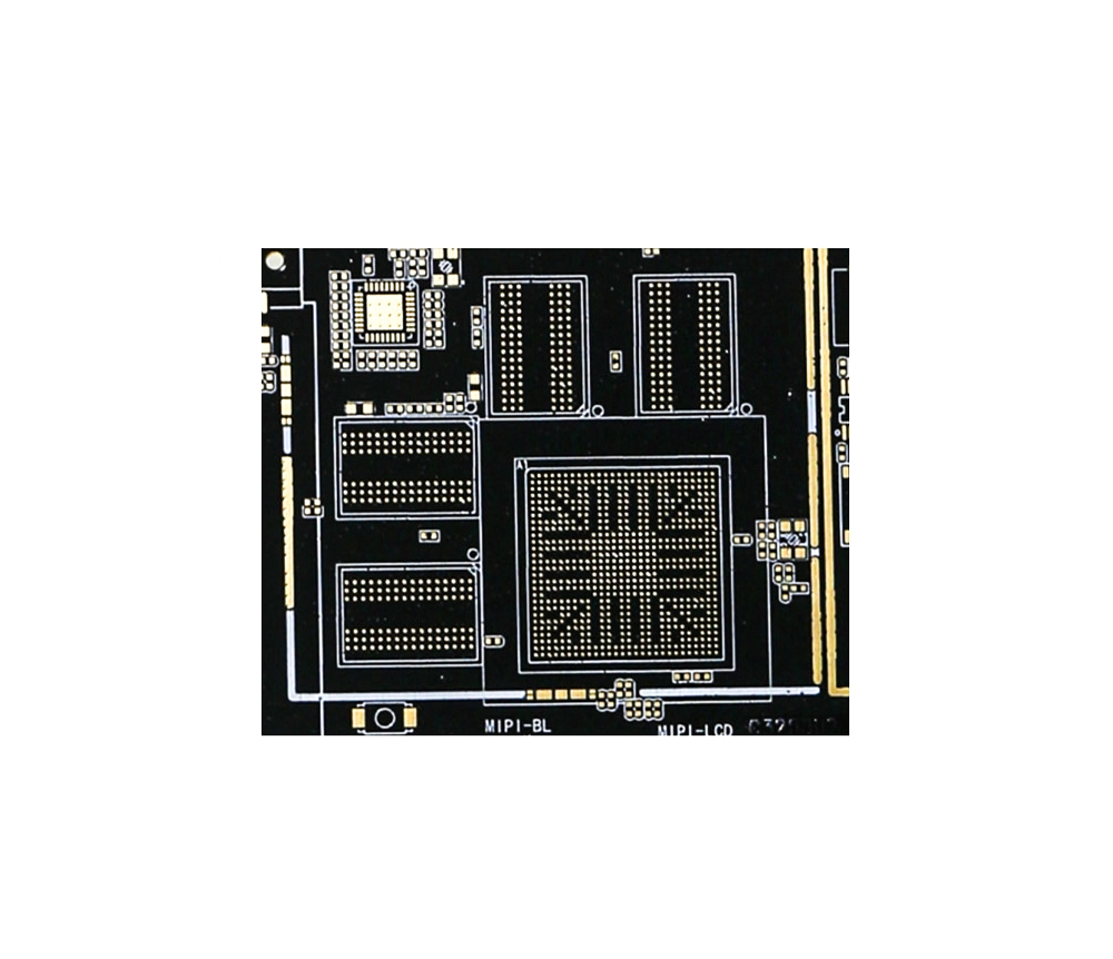
Classified by the upstream and downstream of the industrial chain, it can be divided into raw materials - copper clad panels - printed circuit boards - electronic product applications. The relationship is simply expressed as: fiberglass cloth: fiberglass cloth is one of the raw materials of copper clad panels, made from fiberglass yarn weaving, accounting for about 40% (thick plate) and 25% (thin plate) of the cost of copper clad panels. Glass fiber yarn is made by calcining raw materials such as silica sand in a kiln into a liquid state. It is then pulled into extremely fine glass fibers through extremely small alloy nozzles, and then hundreds of glass fibers are twisted into glass fiber yarn. The construction investment of kilns is huge, usually requiring billions of funds, and once ignited, production must be uninterrupted 24 hours a day, resulting in huge exit costs. Fiberglass fabric manufacturing is similar to weaving enterprises in that it can control production capacity and q
Inquiry Now

