Call Us Now! KnownPCB +86 755 2794 4155 KnownPCB sales@knownpcb.com
Shenzhen KNOWNPCB Technology Co., Ltd.

prototype pcbs

KnownPCBEN KnownPCBCN
KnownPCB
prototype pcbs中文
KnownPCB
News News

News

Home > 
  • News
  • Company News Industry News FAQ

    How LED light work? Learn more about LED board

    How LED light work? Learn more about LED board

    Have you noticed that now more and more of our lighting is using led lighting.What is LED? Compared to the traditional light bulbs, LEDs have lower power consumption, longer lifetime and higher energy efficiency. In the PCB industry,when we say LED PCB, it refers to the pcb used for LED lighting, if you are looking for a suitable LED PCB for your lighting system, this article may bring you something. WHAT ARE LEDS COMPOSED OF?LED is an initial light-emitting diode that produces light when an electric current passes through. LEDs typically have negative and positive electrodes, which generate light in the visible light region.The LEDS are glued to the PCB by soldering process and have electrical connections for lighting.Since light-emitting diodes dissipate a lot of heat when they are in use, when you are designing LED, the metal core is usually the best choice for LED PCB, it is because that it dissipates heat more faster. Among them, the metal material aluminum is the most widely used

    Know Detail

    PCB copper.PCB Assembly for Wireless Communication

    PCB copper.PCB Assembly for Wireless Communication

    Jun 07,2023

        1. If there are many land in PCB, there are SGND, Agnd, GND, etc., and according to the different positions of the PCB board surface, you should use the main "ground" as the benchmark reference to cover the copper. Digital ground and simulation are separated to cover copper. Before the copper is covered, the corresponding power connection is first thicken: 5.0V, 3.3V, etc. In this way structure.  2. For single -point connections in different places, the method is to connect through 0 Euro resistance, magnetic beads or inductance;  3. Copper crop near the crystal, the crystal in the circuit is a high -frequency transmission source, the method is to surround the crystal correction copper, and then the crystal shell is grounded separately.  4. If the island (dead area) problem, if it feels very large, it will not take much money to define a place to add the holes.  5. When starting the wiring, deal with the ground wires, and you should take the ground wire well when you walk. You cann

    Know Detail

    PCB schematic diagram common error.Professional PCB Surface Mount services

    PCB schematic diagram common error.Professional PCB Surface Mount services

    Jun 07,2023

        (1) The ERC reports have no access signal:  a. Define the I/O attributes for the pipeline when creating packaging;  b. Modify the inconsistent GRID attributes when creating an element or placing an element.  c. When creating components, the direction of PIN is reverse, and it must be unconnected in the PIN NAME end.  d. The more common reasons are that there are no engineering documents. This is a mistake that beginners make.  (2) Components run outside the drawing industry: No components are created in the component library diagram table paper center.  (3) The created engineering file network table can only be partially transferred to the PCB: when generating Netlist, no selection is Global.  (4) When using multiple parts created by yourself, do not use Annotate.

    Know Detail

    Common errors in PCB.China Multilayer Printed Circuit Board

    Common errors in PCB.China Multilayer Printed Circuit Board

    Jun 07,2023

        (1) Report node when the network is loaded, not found  a. The components in the schematic diagram use the package that is not available in the PCB library;  b. The components in the schematic diagram use the name of the name in the PCB library inconsistently packaging;  c. The components in the schematic diagram use the PIN Number in the PCB library inconsistent packaging. For example, the triode: Pin Number in SCH is E, B, C, and PCB is 1, 2, 3.  (2) You can never print it on a page when printing  a. No at the original point when creating the PCB library;  b. Move and rotate components multiple times, and there are hidden characters outside the PCB board. Select all hidden characters, reduce PCB, and then move the character to the boundary.  (3) The DRC report network is divided into several parts:  It means that this network is not connected, read the report file, and select the Connected Copper to find.  If it is more complicated, try not to use automatic wiring.

    Know Detail

    How to prevent circuit board warping?Standard PCB Layout and Design Services

    How to prevent circuit board warping?Standard PCB Layout and Design Services

    Jun 07,2023

        1. Engineering Design  The arrangement of interlayer semi cured sheets should correspond; Multi layer core boards and semi cured sheets should use the same supplier's products; The outer C/S surface graphics area should be as close as possible, and independent grids can be used;  2. Drying board before cutting  Generally, at 150 degrees Celsius for 6-10 hours, the moisture inside the board is removed, further allowing the resin to cure completely and eliminating stress inside the board; Drying the board before opening, both the inner layer and both sides are required!  3. Attention should be paid to the warp and weft directions of the cured sheet before laminating the multi-layer board  The shrinkage ratio in the warp and weft directions is different, so pay attention to distinguishing the warp and weft directions before cutting and stacking the semi cured sheet; When cutting the core board, attention should also be paid to the warp and weft directions; The general direction of the

    Know Detail

    The solderability of circuit board holes affects welding quality.PCB Assembly for Power Testing Equipment

    The solderability of circuit board holes affects welding quality.PCB Assembly for Power Testing Equipment

    Jun 07,2023

        Poor solderability of circuit board holes will result in solder defects, affecting the parameters of components in the circuit, leading to unstable conduction of multi-layer board components and inner wires, and causing the entire circuit function to fail. The so-called weldability refers to the property of the metal surface being wetted by molten solder, which means that the solder forms a relatively uniform and continuous smooth adhesive film on the metal surface. The main factors affecting the solderability of printed circuit boards are: (1) the composition of the solder and the properties of the soldered material. Solder is an important part of the welding chemical treatment process. It consists of chemical materials containing flux. The commonly used low melting point eutectic metal is Sn Pb or Sn Pb Ag. The impurity content should be controlled in proportion to prevent the oxide produced by impurities from being dissolved by flux. The function of solder is to help wet the sur

    Know Detail

    The design of circuit boards affects welding quality.Lithium Battery Charger Board Circuit Protection.PCB Assembly for In-vehicle Electronic Equipment.Standard PCB Layout and Design Services

    The design of circuit boards affects welding quality.Lithium Battery Charger Board Circuit Protection.PCB Assembly for In-vehicle Electronic Equipment.Standard PCB Layout and Design Services

    Jun 07,2023

        In terms of layout, when the circuit board size is too large, although welding is easier to control, the printed lines are longer, the impedance increases, the noise resistance decreases, and the cost increases; Over time, the heat dissipation decreases, making it difficult to control welding and prone to interference between adjacent lines, such as electromagnetic interference from circuit boards. Therefore, it is necessary to optimize PCB board design: (1) shorten the wiring between high-frequency components and reduce EMI interference. (2) Components with large weight (such as exceeding 20g) should be fixed with brackets and then welded. (3) Heating elements should consider heat dissipation to prevent significant surface damage Δ If defects occur and rework occurs, the thermistor should be kept away from the heat source. (4) The arrangement of components should be as parallel as possible, which is not only aesthetically pleasing but also easy to weld, making it suitable for mass

    Know Detail

    Why do PCB boards need to be tested?

    Why do PCB boards need to be tested?

    Jun 06,2023

       Firstly, during the production and processing of PCB boards, there will be a certain proportion of defective products. At this point, we need to use mechanical equipment to inspect and screen out unqualified defective products. Therefore, we need to conduct electrical testing. So, what is the difference between testing and flying needle testing?  The testing is divided into test fixture testing and flying needle testing,  In terms of speed, the test frame test will be faster, and the flying needle test will be slower  In terms of cost, the cost of testing racks is higher  As for which testing method to choose, we need to choose based on the number of PCBs. For those with a large number, choose a testing rack, and for those with a small number, choose flying pins  Based on cost, time efficiency, and comprehensive evaluation and selection

    Know Detail

    Where is the profit direction of new energy vehicles in PCB?

    Where is the profit direction of new energy vehicles in PCB?

    Jun 06,2023

        In the automotive market, new energy vehicles have become a rising star, and every car company has launched their own new energy vehicles, which is enough to show that new energy vehicles are the trend and will inevitably enter thousands of households. However, every development process is always full of uncertainty, and there are always new problems waiting to be solved. Whether the subsidy policy for new energy is reasonable, how new energy can smoothly enter the market, and how to avoid new energy safety accidents... In the process of exploring and advancing, new energy vehicles have faced a series of problems thrown by the market. Now, the editor of the circuit board has learned that with the gradual fading of new energy subsidies, the influx of foreign enterprises, and the arrival of the marketization stage of new forces in car manufacturing, the market has raised a new question for new energy vehicle companies - can they make money by selling new energy vehicles?  The Double

    Know Detail

    What exactly is a PCB board used for

    What exactly is a PCB board used for

    Jun 06,2023

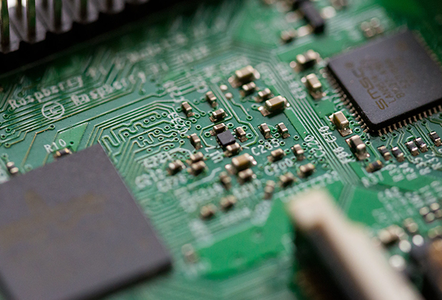
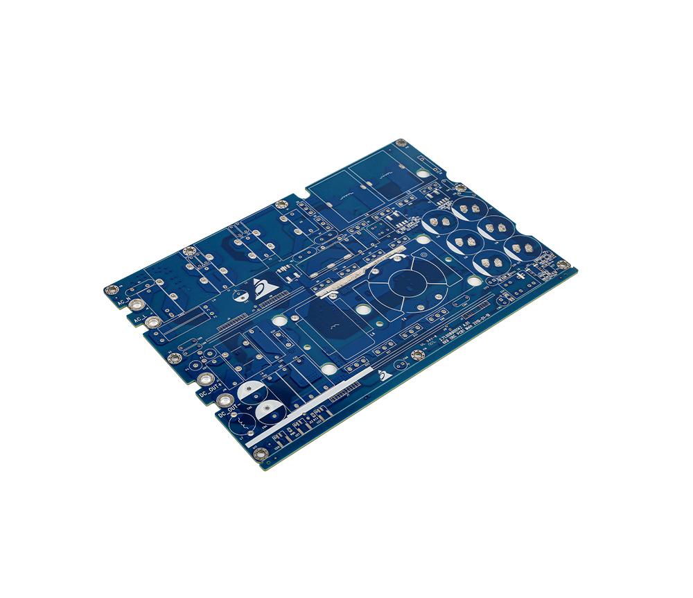
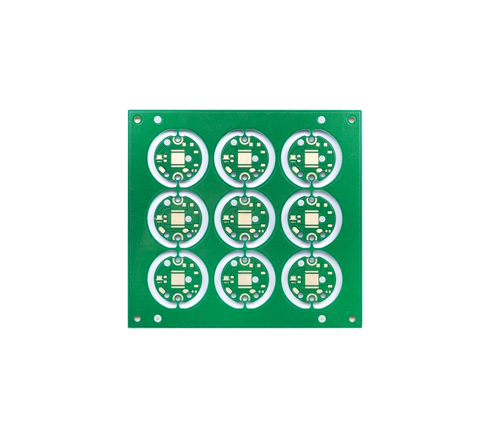
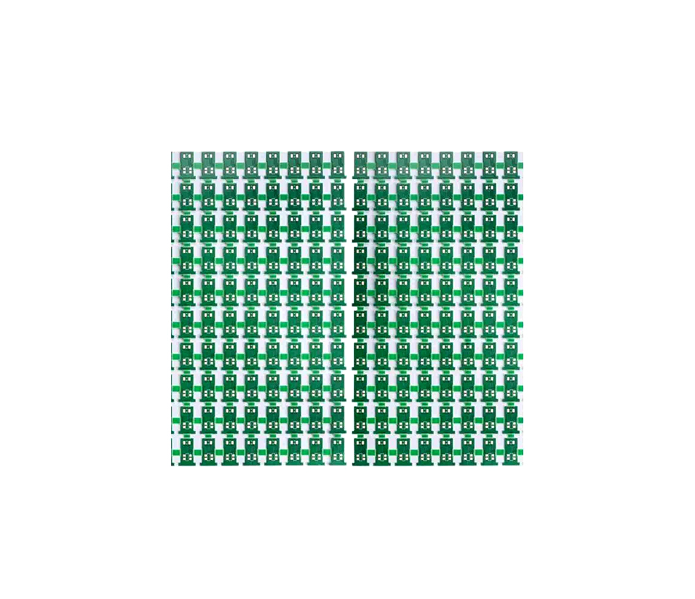
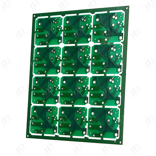
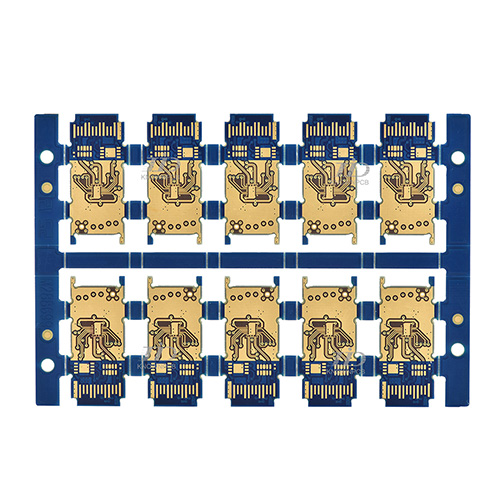
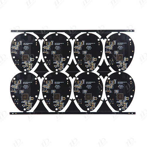
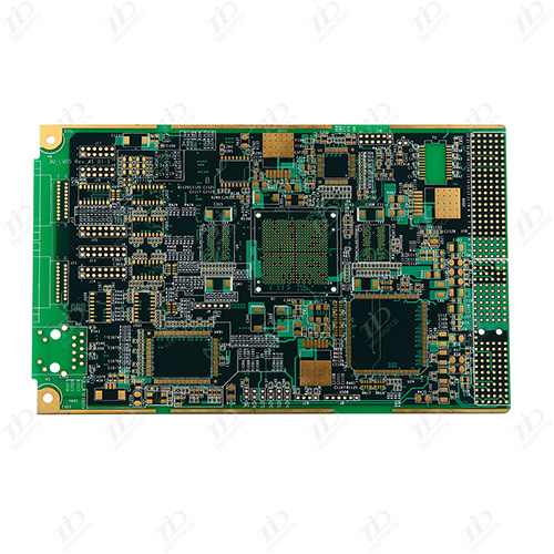
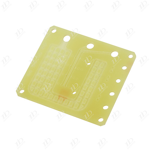
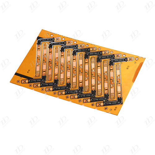
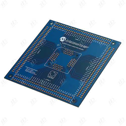
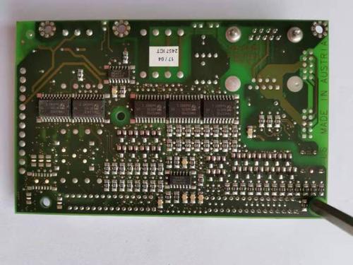
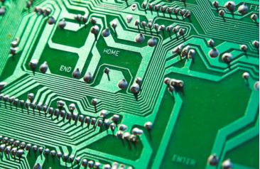
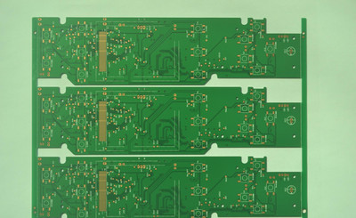
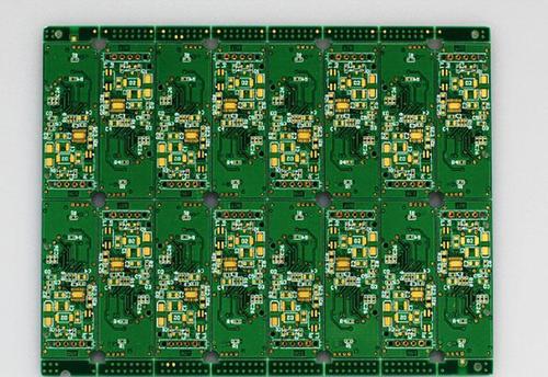
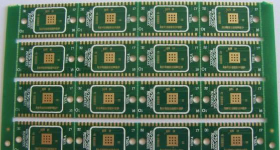
        There are many types of circuit boards with different names, which can be named based on materials, layers, inherent characteristics, and other aspects. For example, there are: single panel, double-sided board, multi-layer board, HDI, fast board, FR4 circuit board, ceramic circuit board, alumina ceramic circuit board, aluminum nitride ceramic circuit board, circuit board, PCB board, aluminum substrate, high-frequency board, thick copper board, impedance board, PCB, ultra-thin circuit board, ultra-thin circuit board, Printing (copper etching technology) circuit boards, etc. Circuit boards are miniaturized and intuitive, playing an important role in the mass production of fixed circuits and optimizing the layout of electrical appliances  Printed circuit boards (PCBs) are essential accessories in modern electronic equipment. All electronic devices, whether they are large machinery, personal computers, communication base stations, mobile phones, household appliances, or electronic toys

    Know Detail

    Multi sensor measurement systems for PCBs are widely favored

    Multi sensor measurement systems for PCBs are widely favored

    Jun 06,2023

        The video measurement system is suitable for measuring prismatic workpieces with intersecting planes. When planes intersect, edges appear, and videos can easily measure edges. Orthopaedic transplantation components are usually composed of continuous and regular curves (artificial hip joint fittings) or complex contour surfaces (artificial knee joint fittings), whose shape is just like the contour of human organ. These surfaces have few or no flat or intersecting edges.  Although video sensors are good at measuring edges and surface points, using a large number of data points to obtain data on even linear cross-sections of contour surfaces is very laborious and impractical. Trigger probes also have the same limitations, as they need to approach each point and return to the plateau after triggering - although feasible, they are also not suitable for measuring large quantities of products.  The best method to determine whether the bionic curve contour of artificial knee joint meets th

    Know Detail

    PCB metal coating

    PCB metal coating

    Jun 01,2023

        In addition to the wiring on the substrate, the metal coating is the place where the substrate line and electronic component are welded. In addition, different metals also have different prices, and different ones will directly affect the cost of production. Different metals also have different weldability and contact, as well as different resistance values, which will directly affect the effectiveness of the component.  Common metal coatings include:  copper  tin  The thickness is usually 5 to 15 μm  Lead tin alloy (or tin copper alloy)  That is welded, the thickness is usually 5 to 25 μm, and the tin content is about 63%  gold  Generally only plated in the interface  silver  Generally, it is only placed in the interface, or the alloy of silver with the whole

    Know Detail

    PCBA overall test

    PCBA overall test

    Jun 01,2023

        Because it is made of electronic printing technology, it is called a "printing" circuit board.  Before the emergence of the printed circuit board, the interconnection between electronic components rely on the wires to directly connect to form a complete line. Circuit bread boards exist only as effective experimental tools, and the printing circuit board has become an absolute dominance in the electronics industry.  At the beginning of the 20th century, in order to simplify the production of electronic machines, reduce the wiring between electronic parts, and reduce the advantages of production costs, they began to study the method of replacing the wiring by printing. In the past thirty years, engineers have continued to propose a metal conductor on the insulating substrate as a wiring. The most successful is that in 1925, Charles Ducas in the United States printed out line patterns on the insulated substrate, and successfully established a conductor to wiring in an electroplating.

    Know Detail

    PCB substrate

    PCB substrate

    Jun 01,2023

        The substrate is generally classified as the insulation part of the substrate. The common raw materials are electric wood plates, glass fiber plates, and various types of plastic plates. The PCB manufacturers generally use an insulating part of glass fiber, non -fabrics, and resin, and then suppressed in epoxy resin and copper foil as "Prepreg".  The common substrates and main ingredients are:  FR-1-phenolic cotton paper, this substrate is commonly referred to as electric wooden boards (higher economy than FR-2)  FR-2 ─ Phenolin cotton paper,  FR-3-Cotton Paper, epoxy resin  FR-4-Woven Glass, epoxy resin  FR-5-glass cloth, epoxy resin  FR-6-f f f, polyester  G-10-glass cloth, epoxy resin  CEM-1-cotton paper, epoxy resin (flame retardant)  CEM-2-cotton paper, epoxy resin (non-flame retardant)  CEM-3-glass cloth, epoxy resin  CEM-4-glass cloth, epoxy resin  CEM-5-glass cloth, polyester  Ain -aluminum nitride  SIC -silicon carbide

    Know Detail

    PCB test development

    PCB test development

    Jun 01,2023

        It is important to develop a steady test strategy to develop a stable test strategy to ensure the compliance and function of designing a stable test strategy to ensure the compliance and function of designing. In addition to the establishment and testing of these complex assembly, the money invested in electronic parts may be very high -when a unit can reach $ 25,000 when the final test is at the final test. Because of this high cost, the problem of finding and repairing assembly is more important than its past and even more important steps. Today, the more complicated assembly is about 18 square inch inch, 18 floors; there are more than 2,900 components on the top and bottom; it contains 6,000 circuit nodes; more than 20,000 welding points need to be tested.  In Langxun Accelerated Manufacturing Factory (N. Andover, MA), manufacturing and testing art -level PCBAs and complete transmission systems. The assembly of more than 5,000 nodes is a concern for us because they are close to

    Know Detail

    PCB through hole technology

    PCB through hole technology

    May 26,2023

        The first PCB uses a hole technology, inserts the hole on one side of the circuit board through the lead, and welded the circuit component to the bronze traces on the other side. The board can be single -sided, with an unpopular component side, or a more compact double panel, welded with components on both sides. By bending 90 degrees in the same direction in the same direction, inserting parts into the circuit board (usually a curved lead on the back of the circuit board), can be installed horizontally with two axial leads (such as resistors, capacitors, and diode). Essence Provide boards in the opposite direction to improve the mechanical strength of parts), welded the lead, and trim the end. The lead can be welded manually or welded with a peak welding machine. Tongkou manufacturing increases the cost of the circuit board by requiring accurate drilling, and limits the available wiring area of the signal wiring on the front of the top layer on the top layer of the top layer of th

    Know Detail

    PCB double panel

    PCB double panel

    May 26,2023

        There are wiring on both sides of Double-Sided Boards. However, to use the wires on both sides, there must be an appropriate circuit connection on both sides. The "bridge" between this circuit is called a guide hole (VIA). The guide hole is a small hole full of metal on PCB, which can be connected to the wires on both sides. Because the area of the double panel is doubled than the single -panel, and because the wiring can be intertwined with each other (it can be around the other side), it is more suitable for more complicated circuits than a single panel. Strictly speaking, double panels are a very important PCB board in the circuit board. His use is very large. Is it easy to watch the PCB board? Make it, the double panel is the extension of one -piece one -piece, which means that the lines of the single -to -surface are not enough to turn to the opposite side. There is also an important feature of the double panel. There is a guide hole. To put it simply, it is double -sided, and

    Know Detail

    PCB's circuit characteristics

    PCB's circuit characteristics

    May 26,2023

        Each trace line is composed of the flat narrow parts of the residual on -carved copper foil. The resistance determined by its width, thickness, and length must be low enough to be carried by the conductor carrier. Power and ground wiring may need to be wider than signal wiring. In the multi -layer board, the entire layer can be mainly solid copper, for ground planes for shielding and power returned. For microwave circuits, transmission cables can be arranged in a plane, such as band lines or micro bands, and their size is carefully controlled to ensure consistent impedance. In radio frequency and fast -switch circuits, the inductance and capacitors of the printing circuit board conductor become an important circuit component, which is usually unwilling; on the contrary, they can be regarded as a conscious part of the circuit design without additional separate components.

    Know Detail

    PCB surface installation technology

    PCB surface installation technology

    May 26,2023

        Surface installation technology appeared in the 1960s, developed a development momentum in the early 1980s, and was widely used in the mid -1990s. Recetishment of the component to make it have a small metal piece or end cover that can directly weld on the PCB surface, rather than the wire through the hole. The component becomes smaller, and the components on both sides of the circuit board are more common than the installation of the hole, allowing smaller PCB components to have higher circuit density. The surface installation is very suitable for highly automation, reducing labor costs and greatly increasing productivity. The components can be installed on the load. The size and weight of the surface installation element can be one -quarter to one -tenth of the hole components, and the passive component is much cheaper. However, the price of semiconductor surface installation devices (SMD) depends more on the chip itself rather than packaging. Compared with larger packaging, there

    Know Detail

    PCB copy of the contact system reliability design

    PCB copy of the contact system reliability design

    May 25,2023

      Correctly selecting the contact material can improve the reliability and life of relay IRF520NPBF. Different relays are different due to the different nature and disconnection capacity of the contact load, and the types and degrees of wear of the contacts are also different; these factors must be taken into account when the design uses contacts and reed materials. The selected contacts and reed materials should meet the following basic requirements:  ① It has good conductivity and thermal conductivity.  ② The contact and plating material should be resistant to arcs or electrical spark wear and mechanical wear, and have a certain hardness and anti -adhesion performance.  ③ The reed material should have good elasticity.  2) Requirements for the design and size design of the contact contact:  ① For small and small loads such as micro -micro, ultra -small, the contacts should be in contact with point contact. PCB copies to increase the pressure on the contact site and destroy pollutants

    Know Detail

    PCB copy value

    PCB copy value

    May 25,2023

        Some people have made such assumptions: If the laptop research takes two years, after studying abroad, we will start to enter research for two years, then in the past two years, we can only sell foreign notebooks. In this way, not only our own laptops are two years later than foreign countries, but in the past two years, the market share and brand effects of foreign laptops in China have reached an indestructible level.  However, if we adopt reverse technology research such as PCB copy board, at the beginning of the laptop, we can quickly keep up with new products research, and we can also add new functions to it for new breakthroughs. In this way, we can be in With its own technological achievements in a short time to compete with foreign monopoly products and quickly surpass.  Specifically, the value of PCB copy is reflected in the following aspects:  From the perspective of an enterprise  Callen can help enterprises quickly update their replacement and keep up with the latest tr

    Know Detail
  • 第一页
  • <
  • 37
  • 38
  • 39
  • 40
  • 41
  • 42
  • 43
  • >
  • Inquiry Now

    small circuit board

    Name *

    Country

    Email *

    Company *

    Phone Number

    Message

    What is the best way to contact you?