 +86 755 2794 4155
  sales@knownpcb.com
-
Shenzhen KNOWNPCB Technology Co., Ltd.
 +86 755 2794 4155
  sales@knownpcb.com
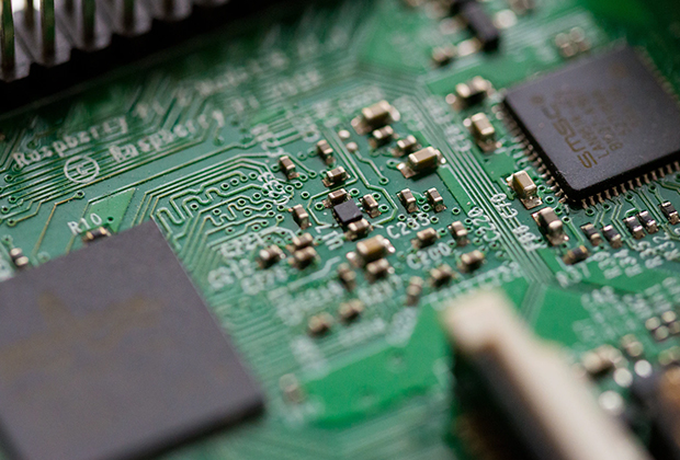
Have you noticed that now more and more of our lighting is using led lighting.What is LED? Compared to the traditional light bulbs, LEDs have lower power consumption, longer lifetime and higher energy efficiency. In the PCB industry,when we say LED PCB, it refers to the pcb used for LED lighting, if you are looking for a suitable LED PCB for your lighting system, this article may bring you something. WHAT ARE LEDS COMPOSED OF?LED is an initial light-emitting diode that produces light when an electric current passes through. LEDs typically have negative and positive electrodes, which generate light in the visible light region.The LEDS are glued to the PCB by soldering process and have electrical connections for lighting.Since light-emitting diodes dissipate a lot of heat when they are in use, when you are designing LED, the metal core is usually the best choice for LED PCB, it is because that it dissipates heat more faster. Among them, the metal material aluminum is the most widely used
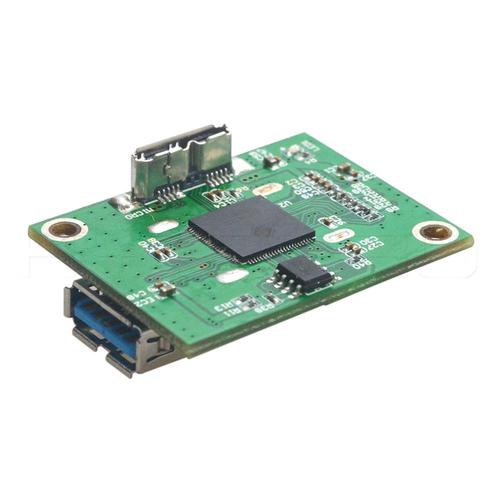
Circuit board design is a "slow work, meticulous work" job, where everyone has their own set of solutions. Below, let the engineer introduce to you the precautions for circuit board design? 1. Circuit board design should have a reasonable direction For example, input/output, AC/ DC, strong/weak signal, high/low frequency, high/low voltage, etc. Their directions should be linear (or separate) and cannot merge with each other. Its purpose is to prevent mutual interference. 2. Choose the appropriate contact position in circuit board design Usually, some commonality is required, such as the multiple grounding wires of the forward amplifier should converge and then be connected to the main line. In fact, due to various limitations, it is difficult to fully achieve this, but this principle should be followed as much as possible. 3. Circuit board design should correctly arrange capacitors Usually only a few power filters/decoupling capacitors are drawn, but it is not indicated where
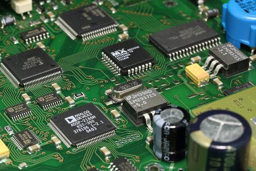
The working environment of circuit boards can be subject to different external disturbances, which may come from power sources, spatial electromagnetic fields, and ground wires. So, what are the measures for suppressing interference on circuit boards? 1. Filter: A filter is a network composed of resistors, inductors, and capacitors with lumped or distributed parameters, used to separate noise superimposed on useful signals. The filter has a good effect on suppressing transient noise of inductive loads, and connecting the power input to the filter can reduce electromagnetic interference from the power grid. 2. Shielding: Shielding refers to the absorption or reflection of external electromagnetic interference by various shielded objects to prevent noise intrusion; Alternatively, limit the electromagnetic energy radiated inside the device to prevent interference with other devices. 3. Reasonable wiring: The type of wire, the thickness of wire diameter, the way of wiring, the dist
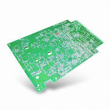
Many customers often overlook many key points when seeking circuit board manufacturers for circuit board sampling, resulting in unsatisfactory circuit board samples and unnecessary losses. So, what are the key considerations for circuit board sampling? 1. Quality The first thing to note is the quality of the circuit board. The selection of boards, the use of ink, production equipment, and the rigor of staff all affect the final quality of circuit boards. 2. Delivery date Customers have all had this experience: the circuit board manufacturer promised delayed sample delivery and found various reasons. Circuit board manufacturers can greatly improve production efficiency and ensure delivery speed only by implementing strict process management during the production process. 3. Price The customer is also very concerned about the price of circuit board samples. The factors that affect the price are the number of layers, thickness, material, order quantity, surface treatment process
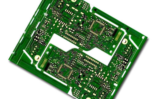
Double panel is a type of circuit board product that customers make a lot. So, how to design a regular double-sided circuit board? Let Shenzhen Circuit Board Factory provide you with a detailed explanation: 1. The common design is that the surface layer is power supply+signal, and the bottom layer is ground+signal. The power supply and ground can adopt a cross bus structure or a large area of copper coating, depending on the actual wiring space. 2. Another good design idea is to implement each layer according to the design requirements of a single panel, and then further adjust and optimize it, such as thickening the power supply/ground wire, and laying copper on large areas of spare parts. 3. When manually wiring, it is necessary to follow some general design guidelines: try to use a ground plane as the current circuit, and separate the analog ground plane from the digital ground plane. If the ground plane is separated by signal wiring, in order to reduce interference with the
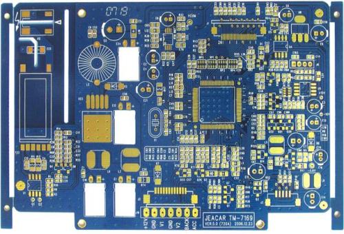
Circuit boards have many "layers", and many beginners are easily confused by various layers of circuit boards when learning circuit board design. Below, let the engineer summarize the definitions of various layers in circuit board design for you to help you better understand and master. 1. Mechanical layer Usually used to place indicative information about circuit boards and assembly methods, such as circuit board dimensions, size markings, data, assembly instructions, and other information. 2. Occlusive layer Draw a closed area on this layer as the effective area for wiring, which cannot be automatically arranged and routed. 3. Silk screen layer The silk screen layer is a text layer that belongs to the top layer of a circuit board and is typically used to mark the projected contour of components, their labels, nominal values or models, and various annotation characters. 4. Welding layer The solder entry layer is the green part of the printed circuit board. After mapping th
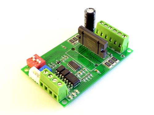
During the design and production process of circuit boards, various problems are always encountered, such as circuit board short circuits, circuit board open circuits, and circuit board solder joints turning golden. Next, let the engineer explain the common problems and cause analysis of circuit board sampling for you in detail. 1. Circuit board short circuit This is one of the common faults in circuit board production, and there are many reasons for this problem: 1) The biggest cause of circuit board short circuits is improper design of welding pads; At this point, the circular welding pad can be changed to an oval shape, increasing the distance between points. 2) Improper design of the direction of circuit board components can also cause short circuits. 3) Automatic plug-in bending foot. It can also cause a short circuit on the circuit board. 4) Other reasons, such as large substrate holes, low tin furnace temperature, poor solderability of the board surface, failure of sol

Circuit board design is a crucial step before circuit board production. So, for beginners, what issues do circuit board design need to understand? Let the engineer share with you: 1. Create packages that are not in the package library. Build using the encapsulation model editor to ensure that the encapsulation model used for the encapsulation library is complete and to ensure the smooth progress of circuit board design. 2. Set circuit board design parameters. According to the needs of circuit system design, set the number of layers, size, color, etc. of the circuit board. 3. Load the network table. Load the web table generated from the schematic diagram and automatically load the component encapsulation model into the circuit board design window. 4. Layout. Combining automatic and manual layout, placing the component packaging model in an appropriate position within the planning range of the circuit board ensures a neat and aesthetically pleasing component layout, which is bene
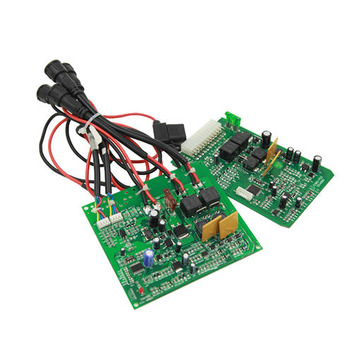
Circuit boards are prone to solder back issues during production, resulting in bending and warping of the board, which affects the product qualification rate. So, how to reduce the risk of bending and deformation in circuit board production? 1. The effect of reducing temperature on the stress of circuit boards. Due to temperature being the main source of stress on circuit boards, as long as the temperature of the reflow furnace is reduced or the production heating speed of the circuit board in the welding furnace is slowed down, the bending and warping of the board can be greatly reduced. 2. The use of boards with higher Tg can increase their ability to withstand stress deformation, but the production cost of circuit boards is also relatively high. 3. Increase the thickness of the circuit board. Many electronic products have circuit board thicknesses of 1.0mm, 0.8mm, or 0.6mm for lighter purposes. It is recommended that if there are no requirements, the circuit board should be 1
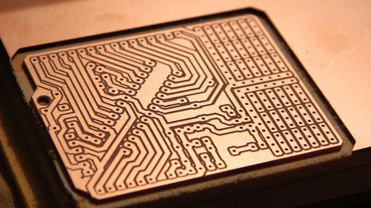
In recent years, with the development of circuit board welding technology, reflow welding technology has become a trend. Below, let Shenzhen circuit board manufacturers explain in detail: What are the three main factors that constitute welding defects in circuit boards? 1. The solderability of circuit board holes affects welding quality The poor solderability of circuit board holes will result in solder defects, affecting the parameters of components in the circuit, causing unstable conduction of multi-layer board components and inner wires, and leading to the failure of the entire circuit function. 2. Welding defects caused by warping of circuit boards The circuit board and components produce warping during the welding process, resulting in defects such as solder joints and short circuits due to stress deformation. Warping is often caused by uneven temperature distribution between the upper and lower parts of a circuit board. In addition, for large-sized circuit boards, they m

1、 Definition of high-frequency PCB circuit board High frequency PCB circuit boards refer to circuit boards with higher electromagnetic frequencies used in the fields of high frequency (frequencies above 300MHz or band lengths not exceeding 1m) and microwave (frequencies above 3GHz or wavelengths not exceeding 0.1m). It is a circuit board produced using ordinary rigid circuit board manufacturing methods or special processing methods on microwave based copper clad plates. Generally speaking, high-frequency circuit boards can be considered as circuit boards with frequencies above 1GHz. With the rapid development of science and technology, many devices are planned to operate in the microwave frequency band (>1GHz) or even millimeter wave (30GHz) range. From this, it can be seen that the frequency is increasing, and the requirements for PCB boards are also high. For example, the substrate material needs to have high-quality electrical properties and chemical stability. With the increas

PCB design is a 'slow work leads to meticulous work' job, where everyone has their own set of solutions. Now let the engineer introduce to you what are the precautions for PCB design? 1. PCB design should have a reasonable direction For example, input/output, AC/ DC, strong/weak signal, high/low frequency, high/low voltage, etc. Their directions should be linear (or separate) and cannot merge with each other. Its purpose is to prevent mutual interference. 2. Choosing a Good Contact Position in PCB Design Usually, some commonality is required, such as the multiple grounding wires of the forward amplifier should converge and then be connected to the main line. In fact, due to various limitations, it is difficult to fully achieve this, but this principle should be followed as much as possible. 3. PCB design should correctly arrange capacitors Usually only a few power filters/decoupling capacitors are drawn, but it is not indicated where they should be placed. In fact, these cap

PCB circuit boards have many "layers", and many beginners are easily confused by various layers of PCB when learning PCB design. Below, let the engineer summarize the definitions of various layers in PCB circuit board design for you to help you better understand and master. 1. Mechanical layer Usually used to place indicative information about circuit boards and assembly methods, such as PCB dimensions, size markings, data, assembly instructions, and other information. 2. Occlusive layer Draw a closed area on this layer as the effective area for wiring, which cannot be automatically arranged and routed. 3. Silk screen layer The silk screen layer is a text layer that belongs to the top layer of a PCB and is typically used to mark the projected contour of components, their labels, nominal values or models, and various annotation characters. 4. Welding layer The solder entry layer is the green part of the printed circuit board. After mapping the shape of the welding layer onto

As a group of engineers, the sampling precautions include: 1. Carefully select the sample quantity to effectively control costs. 2. Special confirmation of device packaging to avoid sample failure due to packaging errors. 3. Conduct a global electrical inspection to improve the electrical performance of the PCB board. 4. Ensure signal integrity layout, reduce noise, and improve PCB stability. As a circuit board sampling manufacturer, the sampling precautions include: 1. Carefully check the PCB file information to avoid data issues. 2. Conduct global process approval and configure the process with our own manufacturers. 3. Control production quantity, reduce costs, and ensure quality. 4. Communicate precautions with sample customers to prevent accidents in advance.
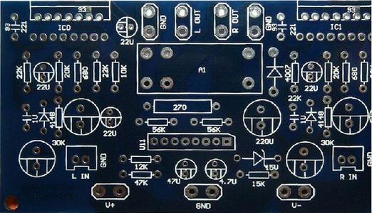
The circuit board manufacturer reveals to you why the circuit board is deformed? The uneven copper surface area on the circuit board can worsen the bending and warping of the board. Nowadays, circuit boards are mostly multi-layer boards, and there are connection points (vias) between layers that are like rivets. The connection points are divided into through holes, blind holes, and buried holes. The places with connection points will limit the effect of board expansion and contraction, and indirectly cause board bending and warping. 1. Generally, circuit boards are designed with a large area of copper foil for grounding purposes. Sometimes, the Vcc layer also has a large area of copper foil. When these large areas of copper foil cannot be evenly distributed on the same circuit board, it will cause uneven heat absorption and dissipation speed. Of course, circuit boards will also expand and contract with heat. If the expansion and contraction cannot be achieved simultaneously, it wi
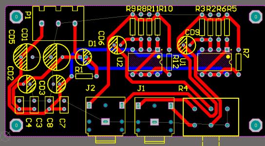
Circuit board sampling refers to the trial production of printed circuit boards before mass production. Generally, it refers to electronic products that are sent to PCB manufacturers for processing after being designed by engineers. The update and iteration of electronic products are relatively fast, so the demand for PCB sampling is gradually growing, and the market share is constantly expanding. With the increasing requirements for electronic product technology and information speed, the rise of multi-layer PCB sampling is relatively fast. 1. There are two ways to sample: formal PCB factories and specialized sample companies. It is more suitable to find a sampling company in your situation. They rely on sampling fees to survive and will definitely accept your request to only make two pieces. 2. The purpose of regular factory sampling is to have bulk orders, so of course, we hope to return orders; The sampling company itself only produces samples or small batches, and even if yo

1 Revenue Both high-frequency circuits and low-frequency power supply circuits have voltage gain and output power harvesting effects. Resonant differential amplification circuit refers to the resonant frequency f0, and for fiber broadband differential amplification circuit, it refers to a frequency range. 2-way band The concept difference with low-frequency power circuit boards is good. For resonant differential amplification circuits, most of them are the values between the two corresponding frequencies when the normalized vibration amplitude of the pointer decreases to 0.707 for the resonant frequency f0; For fiber optic broadband amplification circuits, it refers to the corresponding meaning relative to a certain frequency. 3. Selectivity Selectivity mainly targets resonant amplification circuits, which characterize the circuit's ability to select useful signals and suppress useless signals. Usually, the rectangular coefficient and suppression ratio are measured based on th
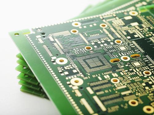
There are five main driving factors for the development of high-performance HDI circuit board products, which affect each other. The factors considered in this type of circuit design are: circuit components (signal integrity), sheet metal, stacking, and design standards. Although circuits are crucial for considering signal integrity, cost factors cannot be ignored. Based on this, it is important to consider a compromise solution during the operation process. The performance of the actual circuit varies with the rise time of the signal. These large area, high-performance HDI circuit boards handle high-speed computer buses or telecommunications signals, and are very sensitive to noise and signal reflection. The following five basic characteristics can describe signal sensitivity: characteristic impedance, low-voltage differential signal (LVDS), signal attenuation, noise sensitivity, and crosstalk interference. The characteristic impedance of single ended microstrip lines, stripline
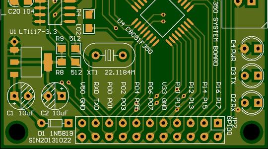
If it is manual welding, it is necessary to develop good habits. Firstly, visually inspect the PCB board before welding, and use a multimeter to check whether key circuits (especially power and ground) are short circuited; Secondly, every time a chip is soldered, use a multimeter to measure whether there is a short circuit between the power supply and ground; In addition, do not throw the soldering iron indiscriminately during soldering. If the soldering tin is thrown onto the solder pins of the chip (especially surface mount components), it is not easy to detect. 2. Open the PCB diagram on the computer, light up the short circuit network, and see where it is closest to where it is most likely to be connected. Pay special attention to internal short circuits in the IC. 3. A short circuit was found. Take a board to cut the thread (especially suitable for single/double layer boards), and after cutting the thread, power on each part of the functional block separately, and exclude som
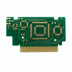
1. Static design Static design refers to the bending or folding that a product only encounters during the assembly process, or the bending or folding that rarely occurs during use. Single sided, double-sided, and multi-layer circuit boards can all successfully achieve folded static design. Usually, for most double-sided and multi substrate designs, the bending radius of the fold should be ten times the thickness of the entire circuit. Circuits with more layers (eight or more) will become very hard and difficult to bend, so there will be no problems. Therefore, for double-sided circuits that require strict bending radius, all copper wires should be set on the same side of the substrate film in the folding area. By removing the film covering on the opposite side, the folded area is approximated as a single sided circuit. 2. Dynamic design The design of dynamic circuits is aimed at the repeated bending that occurs throughout the entire lifecycle of the product, such as the cables o
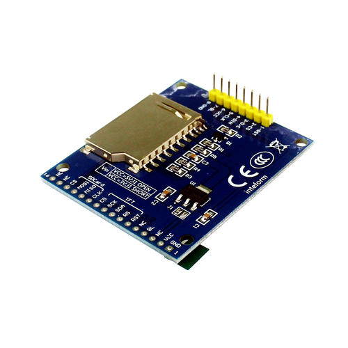
Reduce weight and space Compared to other solutions, flexible printed circuit boards not only provide greater design freedom, but also better space utilization and weight efficiency. Flexible printed circuit boards are thin and lightweight, which can greatly reduce weight and space. For smaller devices, these flexible plates can be folded, creased, and placed in smaller areas to miniaturize the device. This makes flexible circuit boards more suitable for small devices, as they can be installed in areas where rigid circuit boards cannot be installed. flexibility The main advantages of flexible circuit boards are their elasticity and bending ability. Therefore, they can be manipulated in various ways to fit edges, folds, and creases. The flexibility of the circuit board also means that it is more reliable and durable than ordinary PCBs, as it can reduce the impact of vibration and has very few wiring on the circuit board. Minimal wiring eliminates the need for interface connection
Inquiry Now

