 +86 755 2794 4155
  sales@knownpcb.com
-
Shenzhen KNOWNPCB Technology Co., Ltd.
 +86 755 2794 4155
  sales@knownpcb.com
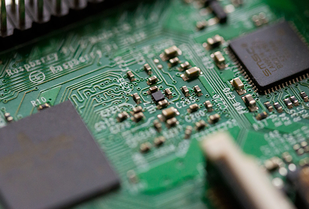
Have you noticed that now more and more of our lighting is using led lighting.What is LED? Compared to the traditional light bulbs, LEDs have lower power consumption, longer lifetime and higher energy efficiency. In the PCB industry,when we say LED PCB, it refers to the pcb used for LED lighting, if you are looking for a suitable LED PCB for your lighting system, this article may bring you something. WHAT ARE LEDS COMPOSED OF?LED is an initial light-emitting diode that produces light when an electric current passes through. LEDs typically have negative and positive electrodes, which generate light in the visible light region.The LEDS are glued to the PCB by soldering process and have electrical connections for lighting.Since light-emitting diodes dissipate a lot of heat when they are in use, when you are designing LED, the metal core is usually the best choice for LED PCB, it is because that it dissipates heat more faster. Among them, the metal material aluminum is the most widely used
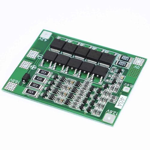
Introduce the relevant content and situation of printed circuit boards to help everyone improve their understanding. Let's read the following content together with the editor. Printed circuit boards (PCBs) are convenient thin sheets used to accommodate interconnected electrical components in a simple, convenient, and economical manner. They are used as physical supports for installing and connecting different electrical components. The PCB is made of glass fiber, composite epoxy resin or any other composite material, and has a metal coated surface. They have etching made of metals and acids to create circuits through different integrated circuits (ICs) and other components on circuit boards. Solder connects ICs and other components to the surface of the circuit board. The copper tracks in the circuit board reduce the possibility of short circuits, misalignment, or misaligned wires. In this way, all components are firmly fixed to the circuit board without the need for complex wir
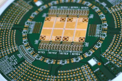
In the field of PCB, there are often many English terms that industry insiders may find difficult to fully recognize. How much do you know about PCB terminology? Let me introduce some commonly used terms in the PCB field to you: 1. FR4 In most cases, the glass fiber substrate for PCBs generally refers to the material "FR4". The solid material "FR4" gives PCB hardness and thickness. Some cheap PCBs are made of materials such as epoxy resin or phenol, lacking the durability of FR4, but they are much cheaper. Phenolic substances have a lower thermal decomposition temperature, and excessive welding time can lead to their decomposition and carbonization, and emit unpleasant odors. 2. Copper The thin copper foil layer on a PCB is pressed onto the substrate through heat and adhesive during production. On double-sided boards, copper foil is pressed onto both sides of the substrate. When we mention "double-sided board" or "two-layer board", we refer to two layers of copper foil on a th
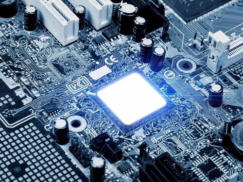
Soft hard combination board refers to a circuit board with FPC and PCB characteristics that is formed by combining flexible circuit boards and hard circuit boards in PCB sampling through pressing and other processes according to relevant process requirements. So, what are the application areas of soft and hard combination boards? 1. Industrial use: including industrial, military, and medical fields. The requirements for soft and hard boards in these fields include high reliability, high accuracy, low impedance loss, complete signal transmission quality, and durability. Due to the complexity of the manufacturing process and low output, the production cost is high. 2. Mobile phone: The application of a soft and hard combination board in a mobile phone, commonly including the turning point of a foldable phone, image module, buttons, and RF module. 3. Consumer electronics products: The software and hardware boards used in DSC and DV are the most representative. In terms of performan
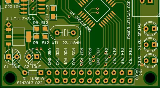
Copper clad laminate (CCL) is the most widely used and important basic board for PCB sampling; It consists of three parts: copper foil, reinforcing material, and adhesive. Its function is to support various components and achieve electrical connections or insulation between them. So, what are the classifications of PCB foil plates? 1. Classification by reinforcement material The most commonly used reinforcement materials for laminated sheets are alkali free, fiberglass products, or paper. Therefore, laminates can be divided into two categories: glass cloth based and paper based. 2. Classification by adhesive type The main adhesives used for laminated sheets include phenolic, epoxy, polyester, polyimide, polytetrafluoroethylene resin, etc. Therefore, laminated sheets are also divided into phenolic, epoxy, polyester, polyimide, and polytetrafluoroethylene laminated sheets accordingly. 3. Classification based on substrate characteristics and usage According to the degree of comb

The so-called copper coating refers to using the idle space on the PCB as a reference plane, and then filling it with solid copper. These copper areas are also known as copper filling. Copper coating can be divided into large-area copper coating and grid copper coating. Next, let professional PCB manufacturers provide you with a detailed understanding of the basic knowledge of PCB circuit board copper coating: 1、 Precautions for copper coating: 1. Single point connection in different locations: connected through a 0 ohm resistor, magnetic bead, or inductor. 2. The copper coating near the crystal oscillator is used as a high-frequency emission source in the circuit. The crystal oscillator should be surrounded by copper coating, and then the outer shell of the crystal oscillator should be grounded separately. 2、 What are the benefits of copper coating? 1. Copper coating can reduce ground wire impedance and improve anti-interference ability; 2. Reduce voltage drop and improve po
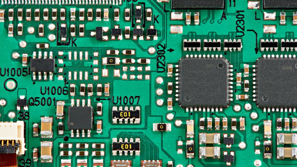
The reasons for the warping of printed circuit boards are, on one hand, the possible warping of the substrate used, and on the other hand, the warping caused by thermal stress, chemical factors, and improper processing during the processing. So, what are the preventive measures for warping of printed circuit boards? 1. Prevent improper inventory methods from causing substrate warping. (1) During the storage process, if the humidity in the inventory environment is high, the copper clad plate will increase warping due to moisture absorption. So for copper clad panels without moisture-proof packaging, attention should be paid to warehouse conditions, minimize warehouse humidity, and avoid bare placement of copper clad panels. (2) Improper placement of copper clad panels can increase warping. If placed vertically or with heavy objects pressed on the copper clad plate, it will increase the warping deformation. Solution: Improve the storage environment, eliminate vertical placement,
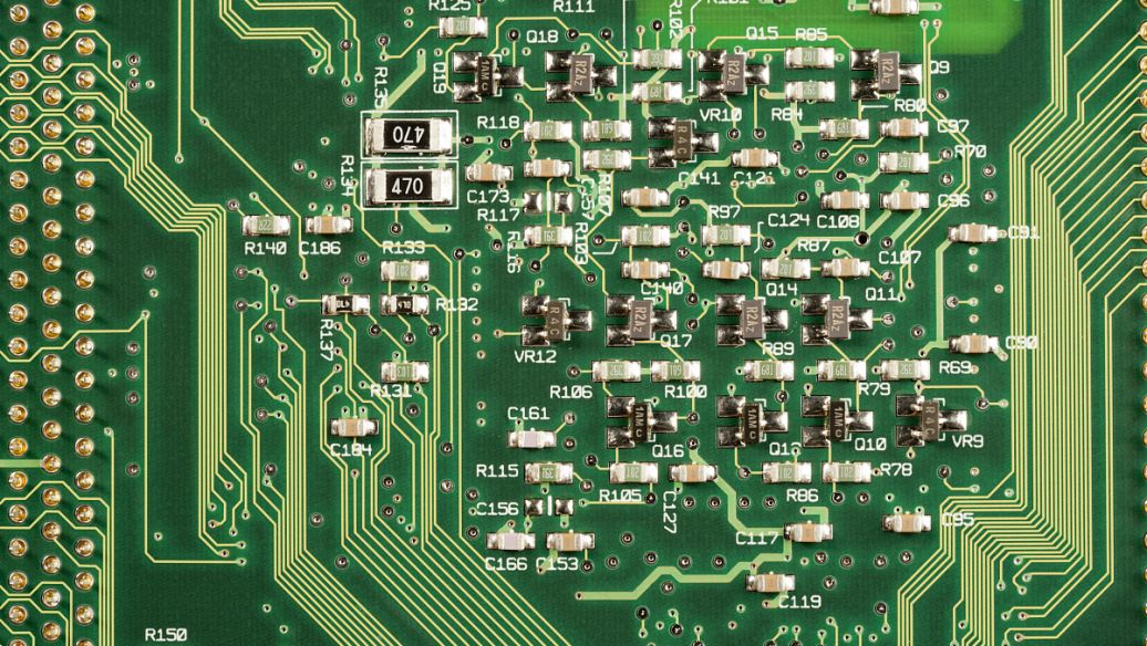
PCB wiring is very important and has a significant impact on the product's lifespan, stability, and electromagnetic compatibility. If the wiring of the circuit board is unreasonable, the product performance will be greatly reduced. Below, we will introduce several special methods for PCB circuit board wiring, hoping to be helpful to you. 1. Right angle wiring: The impact of right angle routing on signals is mainly reflected in: (1) Corners can be equivalent to capacitive loads on the transmission line, slowing down the rise time; (2) Impedance discontinuity can cause signal reflection; (3) The EMI generated by the right angled tip will become a focus of high-speed circuit design in the field of RF design above 10GHz. 2. Differential wiring The advantages of differential signal compared to ordinary single ended signal wiring are as follows: (1) Strong anti-interference ability. Because the coupling between two differential routing lines is good, when there is external noise
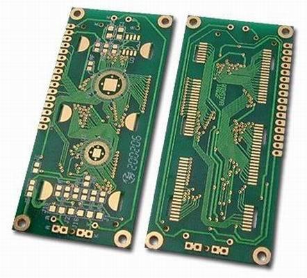
PCB design is particularly important as it appears in almost every electronic device. So, what are the common mistakes in PCB circuit board design? 1、 Character shuffling Including character cover solder pads and SMD solder pads, which brings inconvenience to printed board testing and component welding; The character design is too small, making it difficult to screen, and it can cause characters to overlap and be difficult to distinguish. 2、 Abuse of graphic layers 1. Some useless connections were made on some graphics layers. 2. When designing, it is easy to draw and label the lines that are common to each layer using the Board layer. However, when conducting photo data, the circuit is broken due to missing lines due to the absence of a Board layer. 3、 Overlap of pads 1. The overlap of solder pads (excluding surface mounted solder pads) means the overlap of holes, which can cause damage to the holes during the drilling process due to multiple drilling at one location. 2. T
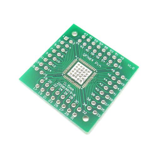
PCB is the fundamental electronic component of all electronic circuit designs, and the design of PCB circuit boards is also a must for engineers to understand. So, what methods should be mastered in PCB circuit board design? 1. There should be a reasonable direction The best direction is in a straight line, but it is generally not easy to achieve, and the most unfavorable direction is in a circular shape. For input/output, AC/DC, strong/weak signals, high-frequency/low-frequency, high-voltage/low-voltage, etc., their direction should be linear (or separated) and should not blend with each other, with the aim of preventing mutual interference. 2. Choose a good grounding point In general, it is required to have a common ground connection, such as: the multiple ground wires of the forward amplifier should be merged and then connected to the main ground, etc. In reality, it is difficult to fully achieve due to various limitations, but efforts should be made to follow them. 3. Reas
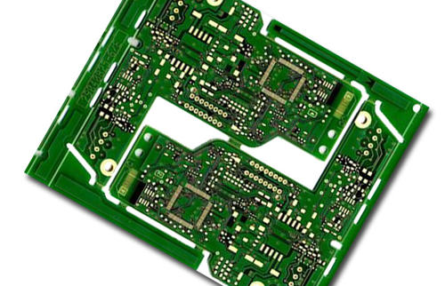
High frequency PCB circuit design is a very complex design process, and its wiring is crucial for the entire design! So, what are the wiring methods for high-frequency PCB circuits? 1. Multilayer board wiring In the PCB layout stage, choose a reasonable number of layers of printed circuit board size, fully utilize the middle layer to set shielding, better achieve nearby grounding, effectively reduce parasitic inductance and shorten signal transmission length, while also significantly reducing signal cross interference. 2. The less bent the leads between electronic device pins, the better It is best to use a full straight line as the lead wire, which requires a turning point. A 45 degree broken line or arc turning point can be used to meet this requirement, but it can reduce the external emission and mutual coupling of high-frequency signals. 3. The shorter the lead between device pins, the better The radiation intensity of a signal is directly proportional to the length of th
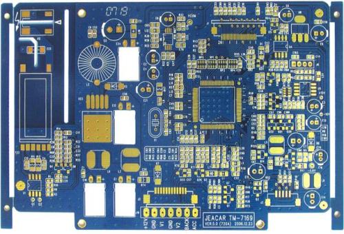
There are significant differences in the usage scenarios, products, performance, materials, areas, and other aspects of PCB boards, resulting in significant changes in the types of components used, the thickness of connecting wires, and the density of wiring. So, what factors need to be considered when selecting PCB boards? 1. For general electronic products, use FR4 epoxy glass fiber substrate; For use with high ambient temperatures or flexible circuit boards, polyimide glass fiber substrates are used; For high-frequency boards, polytetrafluoroethylene glass fiber substrate needs to be used; For electronic products with high heat dissipation requirements, metal substrates should be used. 2. Plates with higher glass transition temperature (Tg) should be appropriately selected, and the Tg value should be higher than the circuit operating temperature. 3. Low coefficient of thermal expansion (CTE) is required for the board. 4. High heat resistance of the board is required. General
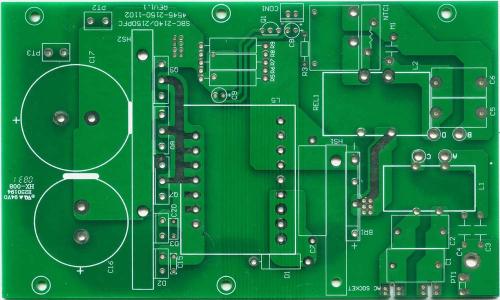
PCB screen printing is an important process in PCB production and also determines the quality of the finished PCB board. So, what are the specifications and requirements for PCB screen printing? 1. All components, installation holes, and positioning holes have corresponding silk screen markings. In order to facilitate the installation of the finished board, the installation holes on the PCB are marked with H1, H2,... Hn by screen printing. 2. Silk screen characters should follow the principle of going from left to right and from bottom to top as much as possible; For devices with polarity such as electrolytic capacitors and diodes, try to maintain consistent orientation within each functional unit. 3. There is no silk screen on the solder pads of the devices and the tin channels that need to be coated with tin, and the device tag number should not be obstructed by the devices after installation; The silk screen should not be pressed on the through hole or solder pad to avoid los
When high-speed PCB wiring is used, the signal will reflect in the transmission channel when the impedance does not match during transmission; The fundamental way to eliminate reflection is to make the impedance of the transmitted signal match well. So, what wiring rules should be followed for impedance matching of high-speed PCB signals? Due to the larger difference between the load impedance and the characteristic impedance of the transmission line, the greater the reflection, it is necessary to make the characteristic impedance of the signal transmission line equal to the load impedance as much as possible; At the same time, it is also important to note that there should be no sudden changes or corners in the transmission line on the PCB, and to try to maintain continuous impedance at each point of the transmission line, otherwise there will also be reflections between different sections of the transmission line. This requires that the following wiring rules must be followed wh
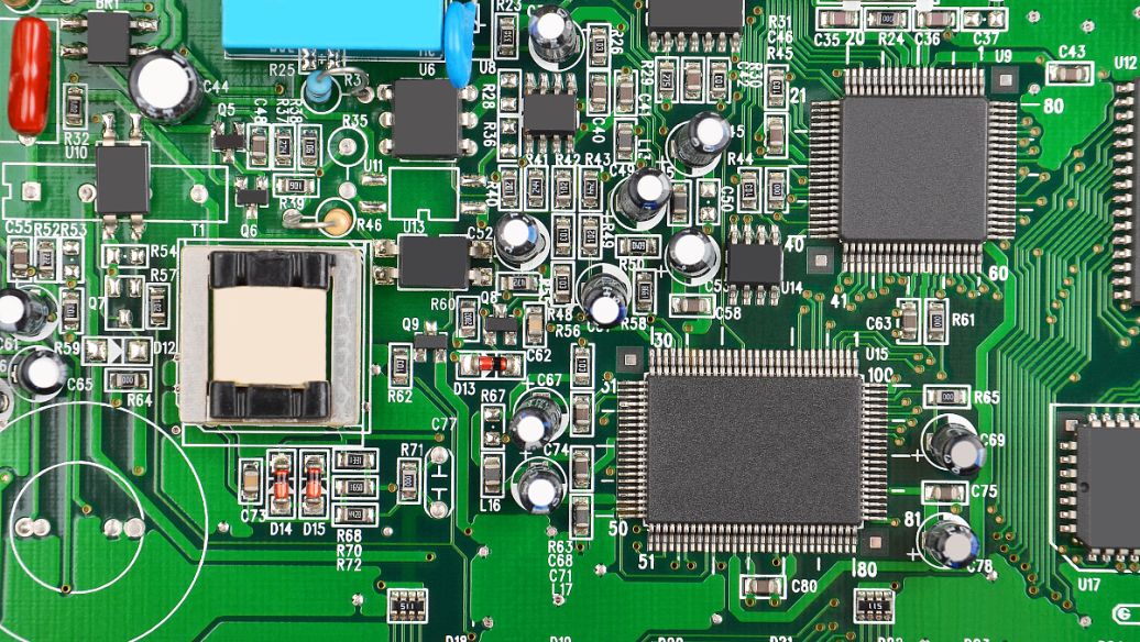
Circuit boards are known as the "mother of electronic components" and are essential basic accessories in electronic devices. Nowadays, there are many circuit board manufacturers on the market. With the development of circuit board production technology, many PCB buyers have gradually begun to understand the basic characteristics of Shenzhen circuit board manufacturers. So, what are the characteristics of excellent Shenzhen circuit board manufacturers? 1、 Having a strong R&D team The reason why Shenzhen circuit board manufacturers are able to produce high-quality circuit boards is that they have a professional research and development team that can provide plasticity suggestions for prototype products in the design stage. In addition, excellent core technical personnel from manufacturers have years of experience in circuit board research and development, which enables them to produce PCB circuit board products with quality assurance strictly in accordance with industry standards a
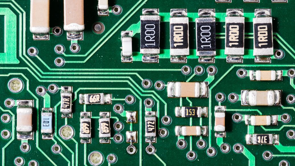
When customers customize PCB products, they always make more in case of unexpected needs. Over time, there may be the phenomenon of PCB boards expiring but being ignored by oneself. So, what are the hazards of using expired PCB circuit boards? 1. Expired PCB may cause oxidation of surface solder pads After oxidation of the solder pad, it will cause poor soldering, which may ultimately lead to functional failure or the risk of parts falling out. The antioxidant effect of different surface treatments on circuit boards may vary, and in principle, ENIG requires that they be used up within 12 months; OSP requires it to be used up within six months, and it is recommended to follow the shelf life of the PCB factory to ensure quality. 2. Expired PCB may absorb moisture and cause board explosion When the circuit board undergoes soldering after moisture absorption, it may cause problems such as popcorn effect, board explosion, or delamination. Although this problem can be solved through
Nowadays, the development of circuit boards is becoming more mature, and their technical level is constantly being updated. A PCB circuit board needs to go through various production processes from prototype to finished product. Sinking process is a commonly used surface treatment process in PCB circuit boards; Next, let the Shenzhen PCB factory take you to understand the process of circuit board gold deposition. The gold deposition process is to deposit a nickel gold coating with stable color, good brightness, flat coating, and good solderability on the surface of PCB printed circuits through chemical reactions; Because of weak adhesion, it is also known as soft gold. Because sinking gold is softer than plating gold, making gold fingers from sinking gold plates is not wear-resistant. The PCB board after sinking gold presents a golden yellow color, which is brighter and more beautiful than the color of gold plating. The Shenzhen PCB factory has summarized its characteristics as fo
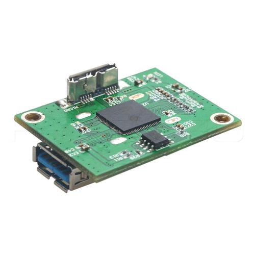
The problem of blackening of the electroplating gold layer often occurs, which affects the quality and performance of the circuit board. So, what are the reasons for the blackening of the electroplating gold layer on PCB board copying? 1. Thickness control of nickel plating layer PCB electroplating gold layer is generally very thin, reflected on the surface of electroplating gold, many of which are caused by poor performance of nickel electroplating. Generally, a thin nickel plating layer can cause the appearance of the product to turn white and black. Generally, it is necessary to electroplate the nickel layer thickness to around 5UM to be sufficient. 2. Condition of plating nickel cylinder solution If the nickel cylinder solution is not well maintained for a long time and carbon treatment is not carried out in a timely manner, the nickel layer electroplated will easily produce flaky crystals, increase the hardness and brittleness of the coating. Serious problems can result in b
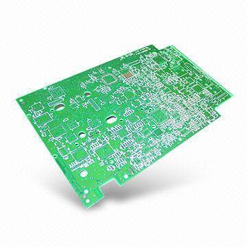
PCBA, which refers to the assembly, mounting, and welding of PCB components, is the core process in PCBA. So, what are the precautions for PCB processing by Shenzhen circuit board manufacturers? 1、 Transportation: To prevent damage to PCBA, during transportation, it is necessary to: 1. Container: Anti static turnover box. 2. Isolation material: anti-static pearl cotton. 3. Placement spacing: There is a distance greater than 10mm between boards and between boards and boxes. 4. Placement height: There is a space greater than 50mm from the top surface of the turnover box. 2、 PCBA processing and washing requirements: 1. Board surface requirements: Clean, with no stains on Wuxi beads and component pins. 2. Devices that should be protected during board washing: wires, connecting terminals, relays, switches, polyester capacitors, and other devices. 3、 Component requirements: All components must not exceed the edge of the PCB board after installation. 4、 Welding requirements: 1.

Printed circuit boards (PCBs) are an indispensable part of electronic devices, and their performance and reliability directly affect the operation of the entire system. PCB (Printed Circuit Board), also known as Printed Circuit Board (PCB) in Chinese, is an important electronic component that supports electronic components and serves as a carrier for the electrical interconnection of electronic components. Due to its use of electronic printing technology, it is called a "printed" circuit board. Cabling is a key step in PCB design, which determines the performance and stability of the circuit board. This article will explore the wiring principles and practical techniques of PCB boards to help engineers achieve better results in design. Wiring principles Following the circuit schematic diagram Wiring should strictly follow the circuit schematic to ensure correct wiring connections and prevent short or open circuit problems. During the wiring process, each component in the circuit
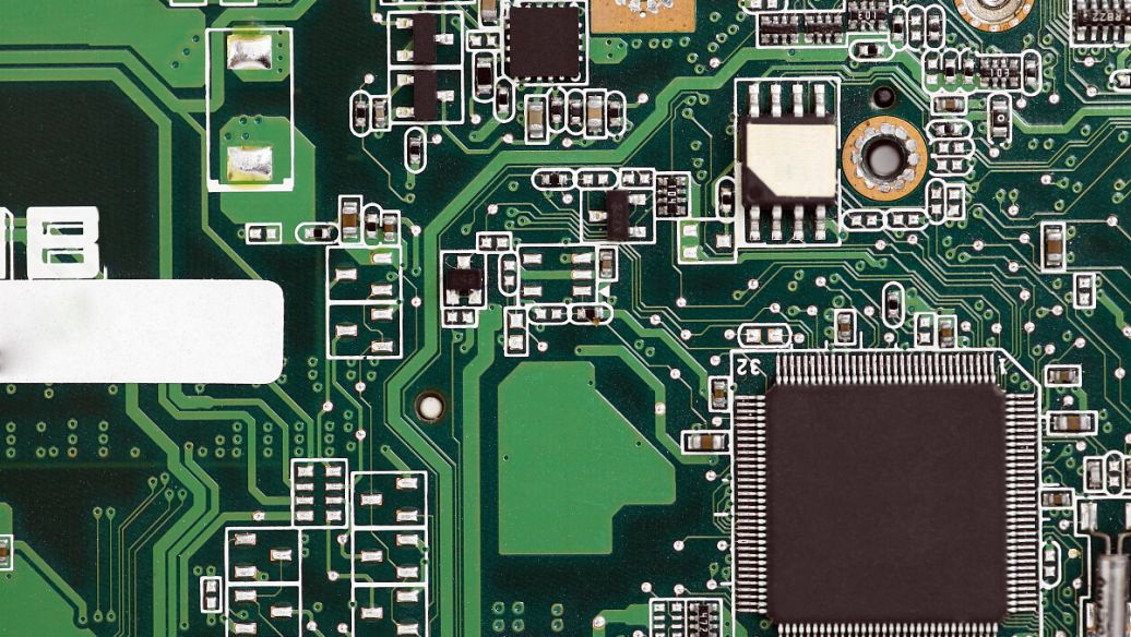
During the production process of PCB circuit boards, due to the inability of printed solder paste and solderless PCB assembly boards to fix the test end of thermocouples, it is necessary to use the actual welded product for temperature testing. So, how to conduct PCB board temperature limit testing? 1、 Select test points: Based on the complexity of the PCB assembly board and the number of channels in the collector, select at least three representative temperature test points that can reflect the high, medium, and low temperatures on the PCB surface assembly board. 2、 Fixed thermocouple: Use high-temperature solder to weld the test ends of multiple thermocouples onto the test points (solder joints), and the solder on the original solder joints must be cleaned before welding; Alternatively, use high-temperature adhesive tape to attach the test ends of the thermocouples to each temperature test point on the PCB. 3、 Insert the other end of the thermocouple into the machine table at
Inquiry Now

