 +86 755 2794 4155
  sales@knownpcb.com
-
Shenzhen KNOWNPCB Technology Co., Ltd.
 +86 755 2794 4155
  sales@knownpcb.com
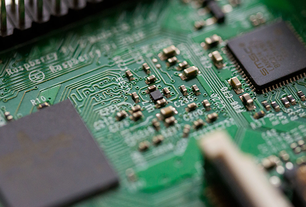
Have you noticed that now more and more of our lighting is using led lighting.What is LED? Compared to the traditional light bulbs, LEDs have lower power consumption, longer lifetime and higher energy efficiency. In the PCB industry,when we say LED PCB, it refers to the pcb used for LED lighting, if you are looking for a suitable LED PCB for your lighting system, this article may bring you something. WHAT ARE LEDS COMPOSED OF?LED is an initial light-emitting diode that produces light when an electric current passes through. LEDs typically have negative and positive electrodes, which generate light in the visible light region.The LEDS are glued to the PCB by soldering process and have electrical connections for lighting.Since light-emitting diodes dissipate a lot of heat when they are in use, when you are designing LED, the metal core is usually the best choice for LED PCB, it is because that it dissipates heat more faster. Among them, the metal material aluminum is the most widely used
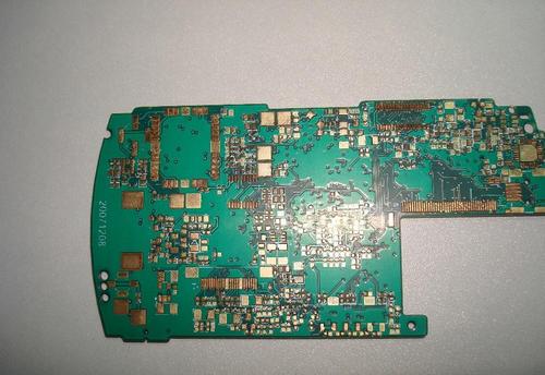
Many HDI circuit boards know that the circuit board industry is a relatively "money burning" industry, and opening a PCB factory is particularly expensive, especially for PCB companies targeting high-end products. The investment in a production line often exceeds 100 million yuan. The largest proportion of investment in PCB factories is in various types of PCB equipment. Take a look at the investment data for the following groups of projects: A major PCB project in Hubei has a total investment of 5 billion yuan, covers an area of 204 acres, and a building area of 240000 square meters, of which 1 billion yuan is invested in equipment. In August 2020, a PCB listed manufacturing enterprise issued convertible bonds to raise a net amount of 1.759 billion yuan to invest in a 1.2 million square meter multi-layer printed circuit board project in Zhuhai, with additional equipment procurement and installation costs of 1.149 billion yuan. The planned investment amount for the first phase
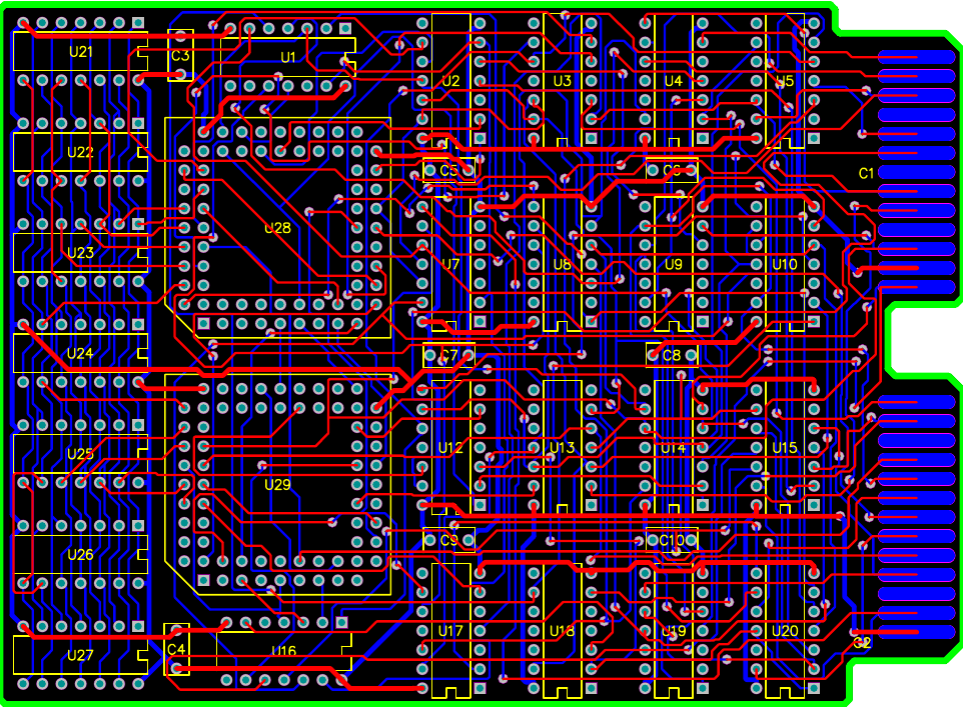
(1) Matching of expansion and contraction coefficients Generally, circuit boards are designed with a large area of copper foil for grounding purposes, and sometimes the Vcc layer also has a large area of copper foil. When these large areas of copper foil cannot be evenly distributed on the same circuit board, it will cause uneven heat absorption and dissipation speed. Of course, circuit boards will also expand and shrink, but if the expansion and contraction cannot match, it will cause different stress changes and ultimately deformation, At this point, if the temperature of the board has reached the Tg value, the board will begin to soften and become permanently deformed after curing. (2) The connection points (vias, vias) of each layer on the circuit board limit the expansion and contraction of the board Nowadays, most circuit boards are multi-layer boards, and there are connection points (through holes, blind holes, buried holes) between layers that are like rivets. In places wh
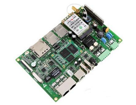
The hole in the pad refers to the hole punched on the pad, which is an SMD pad, usually referring to SMD and BGA pads of 0603 and above, commonly referred to as VIP (via in pad). The solder pad of the plug-in hole cannot be referred to as an in tray hole, as the plug-in hole solder pad requires the insertion of components for welding, and all plug-in pin solder pads have holes. With the development of electronic products in the direction of light, thin, and small, PCB boards have also been pushed towards high-density and difficult development, so the volume of components is gradually decreasing. For example, if the packaging of BGA components is small, the spacing between pins will decrease accordingly. If the pin spacing is small, it is difficult to wire the pins inside the package, and it is necessary to change layers and punch holes for wiring. When the spacing between BGA pins is small and cannot be fanout, there is only one solution, which is to drill holes in the tray. Ther
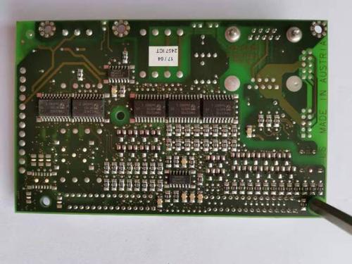
From PCB circuit board design to the completion of all component welding to a high-quality circuit board, it requires strict control from PCB design engineers, as well as the level of welding processes and workers. There are mainly the following factors: PCB board drawing, circuit board workmanship quality, device quality, oxidation degree of device pins, solder paste quality, printing quality of solder paste, accuracy of program programming of the SMT machine, mounting quality of the SMT machine, setting of temperature curve of the reflow soldering furnace, and other factors that may affect poor PCB soldering. The process of PCB drawing is an insurmountable part of the PCB chip welding factory itself. Due to the fact that circuit designers often do not solder circuit boards, they cannot gain direct welding experience and are unaware of the various factors that affect welding; The workers in the welding factory do not understand the drawing board, they only focus on completing pro
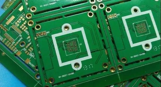
Why sometimes, even though the PCB design has not been checked for errors, there are still adverse situations such as short circuits and broken boards after production and processing? That's because you didn't consider the issue of hole spacing, which resulted in unavoidable losses during the assembly process. The production of a single or double-sided PCB panel involves drilling non through holes or through holes directly after cutting; The multi-layer board is drilled after completing the pressing plate. Drilling can be divided into: part holes, tool holes, through holes, blind holes, and buried holes according to their functions. Conventional drilling is processed through drilling machinery, and in actual processing, the spacing between drilling holes usually affects the processing of the drilling rig and the reliability of the finished product. So when designing, it is important to consider the actual machining situation of hole spacing: VIA via (commonly known as conductiv
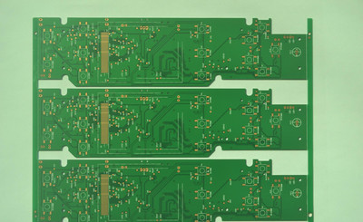
For information on how to best apply DFA, see Why DFA is important for your PCB design and development process. For certain designs, in addition to normal functional testing performed during the prototype phase, testing may also be required. Moreover, this additional test may require you to expand the design to accommodate test equipment, such as adding test points or building test equipment for ROSE testing as needed. For more information about DFT, see Design for Testability (DFT): Do you really need it? For DFR (which should also be included in DFX), the goal is to make design decisions that, once installed and operational, will help improve the reliability performance of the circuit board. These choices will affect the manufacturing, assembly, and components used in your circuit board, as described in the following section.
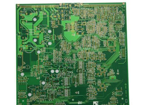
Multilayer circuit board: refers to a printed circuit board with three or more layers of conductive graphics and insulating materials between them, which are laminated and separated, and the conductive graphics between them are interconnected as required. Multilayer circuit boards are a product of the development of electronic information technology towards high speed, multifunctional, large capacity, small volume, thinness, and lightweight. Single sided circuit board: On the most basic PCB, parts are concentrated on one side and wires are concentrated on the other side. Because wires only appear on one side, this type of PCB is called a single sided circuit board. Single panel production is usually simple and cost-effective, but the disadvantage is that it cannot be applied to products that are too complex. Double-sided circuit board: It is an extension of a single panel. When single-layer wiring cannot meet the needs of electronic products, a double-sided board should be used.
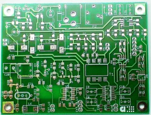
The working principle of a circuit board is to use board based insulation materials to isolate the surface copper foil conductive layer, allowing current to flow along a pre designed route in various components to complete functions such as work, amplification, attenuation, modulation, demodulation, encoding, etc. The circuit board mainly consists of solder pads, vias, mounting holes, wires, components, connectors, thin film circuit SMT patches for Watford circuit boards, SMT patches for thin film circuit SMT patches, fillers, electrical boundaries, etc. The main functions of each component are as follows: Solder pad: A metal hole used for soldering component pins. Through hole: There are metal through holes and non-metal through holes, where metal through holes are used to connect component pins between layers. Installation hole: used to fix the circuit board. Wire: An electrical network copper film used to connect component pins. Connector: A component used for connecting c
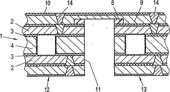
For end users, the ability of your circuit board to perform its expected functions is a basic requirement. More importantly, they remain consistent throughout their expected lifespan. When your design process targets reliability, it is best to achieve this level of performance, including the following. After PCBA is put into operation, its performance will be determined after development and production. The goal of this stage is to ensure that the circuit board always performs its functions or makes it reliable throughout its entire lifecycle. The failure rate of all produced circuit boards is 0%, which is a high standard because circuit boards may encounter unforeseeable situations that are not considered in the design or manufacturing process. Therefore, we should revise our goal to minimize failure rates and maximize service life. Although performance is a post production indicator, it is determined by the measures taken during the development process. An effective PCBA develo

For information on how to best apply DFA, see Why DFA is important for your PCB design and development process. For certain designs, in addition to normal functional testing performed during the prototype phase, testing may also be required. Moreover, this additional test may require you to expand the design to accommodate test equipment, such as adding test points or building test equipment for ROSE testing as needed. For more information about DFT, see Design for Testability (DFT): Do you really need it? For DFR (which should also be included in DFX), the goal is to make design decisions that, once installed and operational, will help improve the reliability performance of the circuit board. These choices will affect the manufacturing, assembly, and components used in your circuit board, as described in the following section.
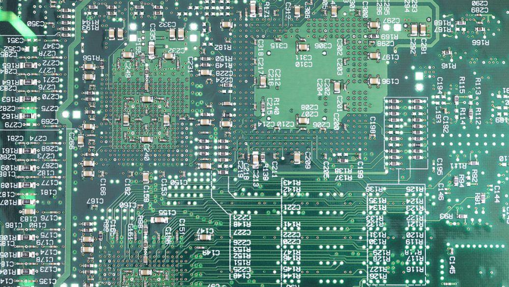
For end users, the ability of your circuit board to perform its expected functions is a basic requirement. More importantly, they remain consistent throughout their expected lifespan. When your design process targets reliability, it is best to achieve this level of performance, including the following. After PCBA is put into operation, its performance will be determined after development and production. The goal of this stage is to ensure that the circuit board always performs its functions or makes it reliable throughout its entire lifecycle. The failure rate of all produced circuit boards is 0%, which is a high standard because circuit boards may encounter unforeseeable situations that are not considered in the design or manufacturing process. Therefore, we should revise our goal to minimize failure rates and maximize service life. Although performance is a post production indicator, it is determined by the measures taken during the development process. An effective PCBA develo
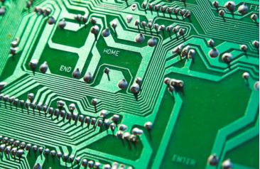
The working principle of a circuit board is to use board based insulation materials to isolate the surface copper foil conductive layer, allowing current to flow along a pre designed route in various components to complete functions such as work, amplification, attenuation, modulation, demodulation, encoding, etc. The circuit board mainly consists of solder pads, vias, mounting holes, wires, components, connectors, thin film circuit SMT patches for Watford circuit boards, SMT patches for thin film circuit SMT patches, fillers, electrical boundaries, etc. The main functions of each component are as follows: Solder pad: A metal hole used for soldering component pins. Through hole: There are metal through holes and non-metal through holes, where metal through holes are used to connect component pins between layers. Installation hole: used to fix the circuit board. Wire: An electrical network copper film used to connect component pins. Connector: A component used for connecting c
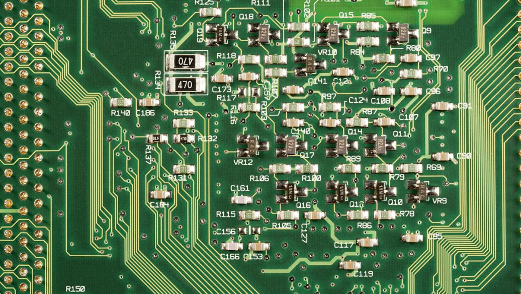
Multilayer circuit board: refers to a printed circuit board with three or more layers of conductive graphics and insulating materials between them, which are laminated and separated, and the conductive graphics between them are interconnected as required. Multilayer circuit boards are a product of the development of electronic information technology towards high speed, multifunctional, large capacity, small volume, thinness, and lightweight. Single sided circuit board: On the most basic PCB, parts are concentrated on one side and wires are concentrated on the other side. Because wires only appear on one side, this type of PCB is called a single sided circuit board. Single panel production is usually simple and cost-effective, but the disadvantage is that it cannot be applied to products that are too complex. Double-sided circuit board: It is an extension of a single panel. When single-layer wiring cannot meet the needs of electronic products, a double-sided board should be used. Bo

On printed circuit boards, all electrical connections of components are made through solder pads. According to different components and welding processes, pads can be divided into two types: non through hole pads and through hole pads. Non through hole pads are mainly used for welding surface mount components, while through hole pads are mainly used for welding pin type components. So, what are the shapes of solder pads? Next, please come with the editor to understand: 1. Circular pad In PCB sampling, circular pads are the most commonly used type of pad. For through-hole pads, the main dimensions of circular pads are the through-hole size and pad size, and the pad size is generally twice the through-hole size. Non through-hole circular pads are mainly used for testing pads, positioning pads, and reference pads, and their main dimensions are pad sizes. 2. Rectangular pad There are two types of rectangular pads: square and rectangular. The square pad is mainly used to identify
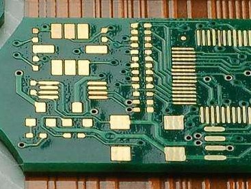
Rigid circuit boards include phenolic paper laminates, epoxy paper laminates, polyester glass felt laminates, and epoxy glass cloth laminates. Flexible printed circuit boards are also known as flexible printed circuit boards or FPCs. Flexible circuit board, also known as FPC or soft board, is a type of printed circuit board that uses polyimide or polyester film as the substrate, has high reliability and flexibility. So, what are the characteristics of flexible circuit boards and rigid circuit boards? 1、 Characteristics of rigid circuit boards: 1. High density. With the improvement of circuit integration and the advancement of mounting technology, high-density printed circuit board technology has become very mature. 2. High reliability. Through a series of inspections, tests, and aging tests, it can be ensured that the PCB works reliably for a long time. 3. Designability. For various performance requirements of PCBs (electrical, physical, chemical, mechanical, etc.), circuit b

Nowadays, the use of PCB multilayer circuit boards on the market has become a popular trend, and in the development of the industry, the ability of many PCB manufacturers to develop and produce PCB multilayer circuit boards has become increasingly prominent. So, what are the requirements for PCB multi-layer circuit board sampling? Below, the editor will analyze for everyone: 1. Requirements for clean appearance. When making samples for PCB multilayer circuit boards, it is necessary to have a flat appearance of the template, no burrs on the edges and corners, and no blistering or delamination between the wires and solder mask. Only in this way can the PCB multi-layer circuit board ensure better welding effect and also ensure that the PCB multi-layer circuit board produced by the PCB manufacturer meets the appearance requirements of actual use. 2. Reasonable process requirements. Before sampling, it is also necessary to study whether the process of PCB multilayer circuit boards is
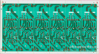
Many customers often confuse rigid flex bonding boards and IC carrier boards. Let a professional PCB factory provide you with a detailed explanation of rigid flex bonding boards and IC carrier boards? 1. What is a rigid flexure composite plate? Rigid flexible combination board refers to the combination of soft and hard boards, which combines a thin layer of flexible and rigid bottom layers, and then presses them into a single component to form a circuit board. It has the characteristics of being flexible and foldable. Due to the mixed use of multiple materials and multiple production steps, the processing time of rigid flexible composite plates is longer and the production cost is higher. In the PCB sampling of electronic consumer products, the use of rigid flexible combination boards not only maximizes space usage and minimizes weight, but also greatly improves reliability, thereby eliminating many demands for welded joints and fragile wiring that are prone to connection proble

Medical PCB board is the supporting part of circuit components and equipment in electronic products. Even if the circuit schematic design is correct or the printed circuit board design is inappropriate, it can have a negative impact on the reliability of electronic products. So design according to certain principles. 1. The principles that should be followed in the layout design of medical PCB boards: Firstly, consider the size of the medical PCB board. When the PCB size is too large, the printing line will be long, the impedance will increase, the noise resistance will decrease, and the cost will increase; If the PCB size is too small, the heat dissipation effect will be poor, and adjacent circuits will be easily disturbed. After determining the size of the printed circuit board, it is also necessary to determine the location of special components. Then, according to the functional units of the circuit, arrange all components of the circuit. When determining the location of speci

So, how to store the half hole PCB board of the module? Circuit boards are not better than other products and cannot come into contact with gases and water. Cannot damage the module half hole PCB vacuum pump. When loading, place a layer of foam pad beside the small box. Bubble pads have better water absorption ability and are very effective in waterproofing. Naturally, waterproof beads are also essential. Then classify and label the sewage. After opening the packaging, the small box must be separated from the wall, stored off the ground in a dry and cool place, and protected from sunlight. Module half hole PCB boards that have undergone metal surface treatment (such as gold immersion, electroplating, tin spray painting, gold plating, etc.) can usually be stored for 6 months, while module half hole PCB boards that have undergone metal surface treatment (such as silver immersion) can usually be stored for 6 months., Tin, OSP, etc. can usually be stored for 3 months. For module half

Module half hole PCB board. A double-layer PCB circuit board is a type of PCB circuit board formed by bonding a replaced conductive pattern layer and an insulating layer material layer. The number of stacked layers of the conductivity pattern is above three, and the interconnection of fixed layer electrical equipment is completed based on metallized holes. If one double-sided board is used as the inner layer, two single-sided aluminum substrates are used as the outer layer, or two double-sided boards are used as the inner layer, and two single-sided aluminum substrates are used as the outer layer, and the raw materials are bonded together according to the system and insulation layer, and the conductivity pattern is interconnected according to the design plan, it becomes a four or six layer PCB circuit board, also known as a double-layer PCB circuit board. A double panel is a material layer in the middle, and both sides are wiring layers. The double-layer module half hole PCB board
Inquiry Now

