 +86 755 2794 4155
  sales@knownpcb.com
-
Shenzhen KNOWNPCB Technology Co., Ltd.
 +86 755 2794 4155
  sales@knownpcb.com
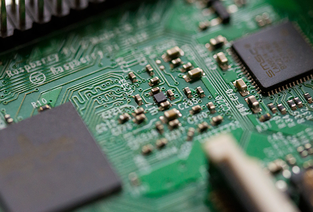
Have you noticed that now more and more of our lighting is using led lighting.What is LED? Compared to the traditional light bulbs, LEDs have lower power consumption, longer lifetime and higher energy efficiency. In the PCB industry,when we say LED PCB, it refers to the pcb used for LED lighting, if you are looking for a suitable LED PCB for your lighting system, this article may bring you something. WHAT ARE LEDS COMPOSED OF?LED is an initial light-emitting diode that produces light when an electric current passes through. LEDs typically have negative and positive electrodes, which generate light in the visible light region.The LEDS are glued to the PCB by soldering process and have electrical connections for lighting.Since light-emitting diodes dissipate a lot of heat when they are in use, when you are designing LED, the metal core is usually the best choice for LED PCB, it is because that it dissipates heat more faster. Among them, the metal material aluminum is the most widely used
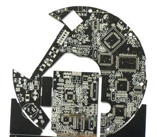
As the speed of integrated circuit output switches increases and the density of PCB boards increases, Signal Integrity has become one of the essential issues in high-speed digital PCB design. Factors such as the parameters of components and PCB boards, the layout of components on the PCB board, and the layout of high-speed signal lines can all cause signal integrity issues. For PCB layout, signal integrity requires providing a circuit board layout that does not affect signal timing or voltage, while for circuit wiring, signal integrity requires providing termination components, layout strategies, and wiring information. High signal speed, incorrect layout of termination components, or incorrect wiring of high-speed signals on a PCB can all cause signal integrity issues, which may result in incorrect system output, abnormal circuit operation, or even complete failure. How to fully consider signal integrity factors and take effective control measures in the PCB design process has b
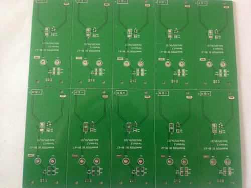
Answer: 1. The circuit board surface includes a foil coated substrate and a pre copper plated substrate after hole metallization. To ensure a firm adhesion between the dry film and the substrate surface, it is required that the substrate surface be free of oxide layers, oil stains, fingerprints, and other dirt, drilling burrs, and rough coatings. To increase the contact area between the dry film and the substrate surface, it is also required that the substrate have a micro rough surface. To meet the above two requirements, the substrate must be carefully treated before applying the film. The treatment methods can be summarized into two categories: mechanical cleaning and chemical cleaning. 2. The same principle applies to resistance welding. Before resistance welding, grinding the plate is to remove some oxidation layers, oil stains, fingerprints, and other dirt from the plate surface. In order to increase the contact area between the resistance welding ink and the plate surface and
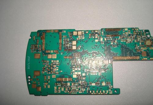
With the continuous enhancement of mobile terminal functions and the continuous development of thinness and lightness, the design of HDI boards is more towards third-order or even any layer HDI boards. Apple has adopted any layer of HDI for the first time in iPhone 4 and iPad 2, significantly improving the product's lightness and thinness. Subsequently, the Android camp quickly followed suit, and any layer of HDI became the standard motherboard for current mid to high-end smartphones. According to statistics, changing from first-order HDI to any layer HDI can reduce the volume by about 40%. It is expected that any layer of HDI will be applied in an increasing number of high-end smartphones and tablets in the future. At present, the adoption rate of third-order HDI and any layer HDI for smartphones is about 30%, while the adoption rate for tablets is even higher at over 80%. We believe that mobile terminals represented by smartphones will continue to drive the development of HDI boa
In addition to mobile terminals, high-end servers will also drive up the overall demand level for HDI. Currently, PCBs with layers below 8 are mainly used for household appliances, PCs, desktop computers, etc., while high-end applications such as high-performance multi-channel servers and aerospace require PCBs with layers above 10. Taking servers as an example, on single or dual channel servers, PCB boards are generally between 4-8 layers, while high-end servers such as 4-way and 8-way require 16 layers or more on the motherboard and 20 layers or more on the backplane. Therefore, HDI boards are more commonly used. The development of the domestic cloud computing market and the rapid expansion of mobile internet such as mobile payments, OTO applications, and social networks have driven the steady growth of the Chinese server market, becoming the main driving force for global shipment growth, and the growth rate is constantly increasing. In 2015, the sales revenue was 49.82 billion
1. Why do I need to plug holes when BGA is in resistance welding? What are the acceptance criteria? Answer: Firstly, the solder plug hole is to protect the service life of the through hole. The hole diameter required for the BGA position plug is generally relatively small, ranging from 0.2 to 0.35mm. During the subsequent processing, some of the medicine in the hole is not easy to dry or evaporate, and it is easy to leave residue. If the solder plug hole is not plugged or not full during the solder plug, there will be residual foreign objects or solder beads in the subsequent processing such as tin spraying and gold deposition, which will be heated when the customer installs the component for high-temperature welding, Foreign objects or tin beads inside the hole will flow out and adhere to the component, causing defects in the performance of the component, such as open circuit or short circuit. BGA is located in the solder plug hole A. Be sure to plug it fully. B. There should be
After several waves of upward momentum, PCB factories have already reached their limits in terms of affordability. It is understood that in the past six months, the average price of CCL materials has increased by about 20-30%. Therefore, most PCB manufacturers, especially traditional hard board manufacturers, can no longer withstand the pressure and have started price negotiations with customers, hoping that customers can understand the pressure from PCB factories and help absorb some costs. The end customers, ODM and OEM factories that are in contact with PCB factories have seen a real shortage of materials, and the pressure to rush out far outweighs the cost pressure. Recently, their attitudes have indeed softened. It is widely believed that although the magnitude of the price increase cannot be determined, the cost transfer negotiations among PCB factories are expected to achieve certain results. Even if the price increase is only 5-10%, it can be considered as a small supplemen

The main purpose of PCB baking is to remove moisture and moisture, removing moisture inside or absorbed from the outside of the PCB, as some PCBs themselves use materials that easily form water molecules. In addition, after PCB production and placement for a period of time, there is also a chance to absorb moisture from the environment, and water is one of the main culprits causing PCB explosion or delamination. Because when the PCB is placed in an environment with a temperature exceeding 100 ℃, such as a reflow furnace, wave soldering furnace, hot air leveling, or manual welding process, water will become water vapor and quickly expand its volume. The faster the heating speed on the PCB, the faster the expansion of water vapor; The higher the temperature, the larger the volume of water vapor; When water vapor cannot escape from the PCB in a timely manner, there is a good chance of expanding the PCB. Especially the Z direction of a PCB is the most fragile, sometimes it may brea
At present, the formation process of refined circuits includes laser imaging (pattern transfer) and pattern etching forming. Laser direct imaging (LDI) technology is the process of obtaining refined circuit patterns directly by laser scanning on the surface of copper clad plates coated with photoresist. Laser imaging technology greatly simplifies the process flow and has become the mainstream technology in HDI PCB plate making. The application of semi additive method (SAP) and improved semi additive method (mSAP), namely graphic etching method, is increasing nowadays. This technology process can also achieve conductive circuits with a line width of 5um. How to improve electroplating uniformity and deep hole plating ability in PCB manufacturing, and improve the reliability of the board. This depends on the continuous improvement of the electroplating process, starting from various aspects such as the proportion of electroplating solution, equipment allocation, and operating proce

With the development of technology, some high-tech devices are becoming increasingly miniaturized and precise, which puts higher demands on the HDI boards they use. The line width/spacing of HDI circuit boards for some devices has evolved from early 0.13 mm (5 mils) to 0.075 mm (3 mils) and has become a mainstream standard. As a leading enterprise in the HDI fast board industry, Shenzhen Benqiang Circuit Co., Ltd. has achieved a production process of 38 μ M (1.5 mil) is approaching the limit of the industry. The increasingly high requirements for line width/distance have brought the most direct challenge to graphic imaging in the PCB manufacturing process. So how are the copper wires on these precision boards processed and formed? The important feature of HDI circuit boards is the presence of micro through holes (aperture ≤ 0.10 mm), all of which belong to buried blind hole structures. The buried blind holes on HDI boards are currently mainly processed by laser, but there are a
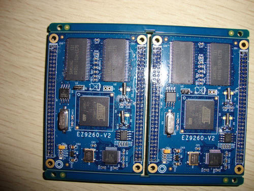
PCB circuit board impedance refers to the parameters of resistance and reactance, which hinder AC power. In the production of PCB circuit boards, impedance processing is essential. The reasons are as follows: 1. PCB circuits (bottom of the board) should consider the installation of electronic components by plugging, and after plugging, issues such as conductivity and signal transmission performance should be considered. Therefore, it is required that the impedance should be as low as possible, and the resistivity should be less than 1&TIMes per square centimeter; Below 10-6. 2. During the production process of PCB circuit boards, they need to go through processes such as copper deposition, electroplating tin (or chemical plating, or thermal spraying tin), and connector soldering. The materials used in these processes must ensure a low resistivity to ensure that the overall impedance of the circuit board meets product quality requirements and can operate normally. 3. The tin plat
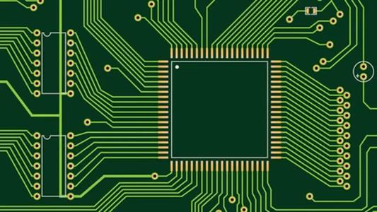
For the electronics industry, according to industry surveys, the most fatal weaknesses of chemical tin plating are its susceptibility to discoloration (i.e. oxidation or deliquescence), poor solderability leading to difficulty in soldering, high impedance leading to poor conductivity or unstable overall board performance, and susceptibility to tin growth, which can lead to short circuits in PCB circuits and even burning or ignition events. It is reported that Kunming University of Technology in the early 1990s was the first to study chemical tin plating in China, followed by Guangzhou Tongqian Chemical (Enterprise) in the late 1990s. It has been recognized in the industry for the past 10 years that these two institutions are doing the best. Among them, according to our contact screening investigations, experimental observations, and long-term endurance tests of numerous enterprises, it has been confirmed that the tin coating of Tongqian Chemical is a pure tin layer with low resist
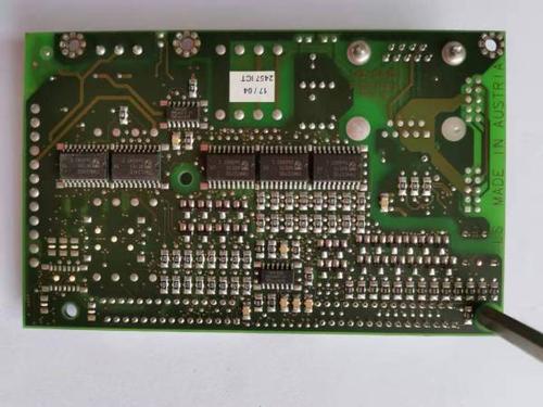
(1) Characteristic impedance In electronic information products such as computers and wireless communication, the energy transmitted in the circuit of a PCB is a square wave signal (pulse) composed of voltage and time, and the resistance it encounters is called characteristic impedance. (2) Differential impedance Two identical signal waveforms with opposite input polarity at the driving end are transmitted by two differential lines, and these two differential signals are subtracted at the receiving end. The differential impedance is the impedance Zdiff between two lines. (3) Odd mode impedance The impedance of one line to ground in the two lines is consistent. (4) Even mode impedance The impedance Zcom of two identical signal waveforms with the same input polarity at the driving end when connecting the two wires together. (5) Common mode impedance The impedance Zoe of one line to ground in the two lines is consistent, usually greater than the odd mode impedance.

1) Single panel process flow Cutting and grinding → drilling → outer layer graphics → (full plate gold plating) → etching → inspection → silk screen welding resistance → (hot air leveling) → silk screen characters → contour processing → testing → inspection 2) Process flow of double-sided tin spraying board Cutting and grinding → drilling → copper sinking and thickening → outer layer graphics → tin plating, etching and tin removal → secondary drilling → inspection → silk screen resistance welding → gold-plated plug → hot air leveling → silk screen characters → external processing → testing → inspection 3) Process flow of nickel gold plating on double-sided boards Cutting and grinding → drilling → copper sinking and thickening → outer layer graphics → nickel plating, gold film removal and etching → secondary drilling → inspection → silk screen resistance welding → silk screen characters → external processing → testing → inspection 4) Process flow of multi-layer tin spraying bo
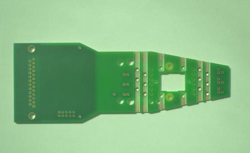
The names of circuit boards include: ceramic circuit boards, alumina ceramic circuit boards, aluminum nitride ceramic circuit boards, circuit boards, PCB boards, aluminum substrates, high-frequency boards, thick copper plates, impedance boards, PCBs, ultra-thin circuit boards, ultra-thin circuit boards, printed (copper etching technology) circuit boards, etc. Circuit boards make circuits miniaturized and intuitive, playing an important role in the mass production of fixed circuits and optimizing the layout of electrical appliances. A circuit board can be called a printed circuit board or a printed circuit board, with the English name "Printed Circuit Board" PCB (Flexible Printed Circuit Board) FPC circuit board (FPC circuit board, also known as flexible circuit board) is a highly reliable and excellent flexible printed circuit board made of polyimide or polyester film as the substrate. It has the characteristics of high wiring density, light weight, thin thickness, and good bending p
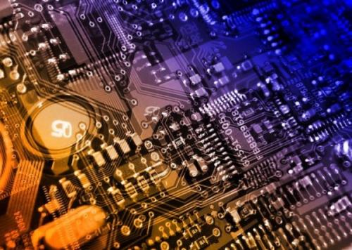
The circuit processing of multi-layer PCBs is no different from that of single-layer and double-layer PCBs, but the biggest difference lies in the through hole process. The circuits are all etched, and the via holes are drilled and then plated with copper. Everyone involved in hardware development understands these, so we won't go into detail. Multilayer circuit boards typically include through hole boards, first order boards, second order boards, and second order stacked hole boards. Higher level boards such as third-order boards and arbitrary layer interconnection boards are rarely used in daily life, and their prices are quite expensive. We won't discuss them much for now. In general, 8-bit microcontroller products use 2-layer through-hole boards; Intelligent hardware at the 32-bit microcontroller level, using 4-6-layer through-hole boards; Intelligent hardware at the Linux and Android levels, using 6-layer through holes to 8-layer first-order HDI boards; Compact products lik
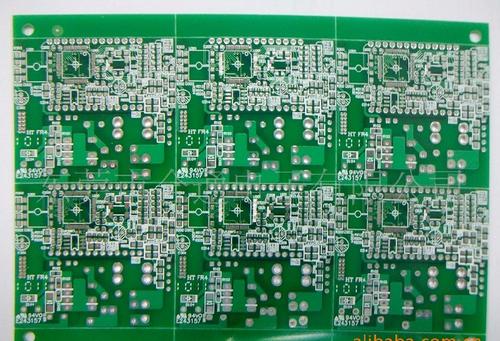
1. The meaning of the solder mask layer is to open a window on the green oil of the entire solder mask, in order to allow welding! 2. By default, areas without solder mask must be coated with green oil! 3. Paste mask layer for SMD packaging! SMT encapsulation uses: toplayer layer, topsolver layer, toppaste layer, and the toplayer is the same size as the toppaste layer, but the topsolver is one circle larger than them. DIP encapsulation only uses the top layer and multi layer layers (after some decomposition, I found that the multi layer layer is actually the top layer, bottomlayer, top layer, and bottomlayer layers with overlapping sizes), and the top layer/bottomlayer is one circle larger than the top layer/bottomlayer. Question: Is the statement 'tin or gold plating only occurs when the copper layer corresponding to the solder layer has copper' correct? This sentence is from a person who works in a PCB factory. His meaning is: to make the effect of tin plating on the part pain

Protel 99 SE provides 16 mechanical layers, which are generally used to set the overall dimensions, data markers, alignment markers, assembly instructions, and other mechanical information of circuit boards. These information may vary depending on the requirements of the design company or PCB manufacturer. Executing the menu command Design | MechanicalLayer can set more mechanical layers for the circuit board. In addition, the mechanical layer can be attached to other layers to output the display together. 4 Solder mask layer Apply a layer of paint, such as solder mask, to various areas outside the solder pad to prevent tin from being applied to these areas. The solder mask layer is used to match the solder pad during the design process and is automatically generated. Protel 99 SE provides two solder mask layers: Top Solder and Bottom Solder. 5 Paste mask layer Its function is similar to that of the solder mask layer, except for the corresponding bonding pads of surface mounted
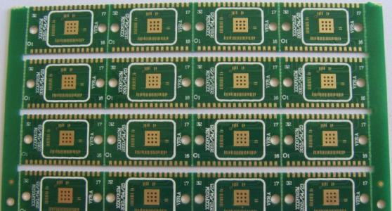
The volume of electronic products is becoming increasingly thin and short, and directly stacking holes on through blind holes is a design method to achieve high-density interconnection. To do a good job of stacking holes, the first step is to ensure the flatness of the hole bottom. There are several production methods, and the electroplating hole filling process is one of the representative ones. Next, let the PCB engineer teach you about the PCB electroplating hole filling process. 1. Advantages of electroplated hole filling: (1) Beneficial for designing stacked holes and holes on the disc; (2) Improving electrical performance helps with high-frequency design; (3) Helps to dissipate heat; (4) Plug holes and electrical interconnections are completed in one step; (5) The blind hole is filled with electroplated copper, which has higher reliability and better conductivity than conductive adhesive. 2. Physical impact parameters The physical parameters that need to be studied in

On PCBs, nickel is used as a substrate coating for precious and base metals. The deposition layer of low stress nickel on PCB is usually prepared using modified Watt nickel plating solution and some amino sulfonic acid nickel plating solution with stress reducing additives. What are the common problems encountered when using PCB nickel plating solution, as analyzed by CITIC Huawei? 1、 Temperature - Different nickel processes use different plating bath temperatures. In nickel plating solutions with higher temperatures, the obtained nickel coating has low internal stress and good ductility. The general operating temperature is maintained at 55-60 degrees Celsius. If the temperature is too high, nickel salt hydrolysis will occur, causing pinholes in the coating and reducing cathodic polarization. 2、 PH value - The pH value of nickel plating electrolyte has a significant impact on the performance of the coating and electrolyte. The pH value of PCB nickel plating electrolyte is genera

The volume of electronic products is becoming increasingly thin and short, and directly stacking holes on through blind holes is a design method to achieve high-density interconnection. To achieve good hole stacking, the first step is to ensure the flatness of the hole bottom. There are several typical methods for making flat hole surfaces, and electroplating hole filling process is one of the representative ones. The electroplating hole filling process can not only reduce the necessity of additional process development, but also be compatible with current process equipment, which is conducive to achieving good reliability. So, what factors affect the PCB electroplating hole filling process? In PCB sampling, the influence of substrate on electroplating hole filling cannot be ignored, generally including factors such as dielectric layer material, hole shape, thickness to diameter ratio, and chemical copper coating. (1) Medium layer material. The material of the dielectric layer ha
Inquiry Now

