 +86 755 2794 4155
  sales@knownpcb.com
-
Shenzhen KNOWNPCB Technology Co., Ltd.
 +86 755 2794 4155
  sales@knownpcb.com
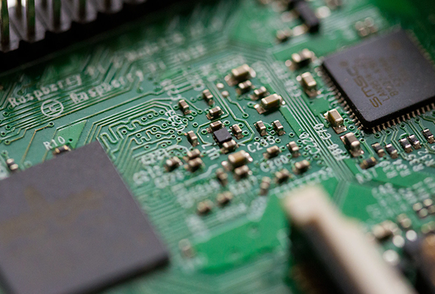
Have you noticed that now more and more of our lighting is using led lighting.What is LED? Compared to the traditional light bulbs, LEDs have lower power consumption, longer lifetime and higher energy efficiency. In the PCB industry,when we say LED PCB, it refers to the pcb used for LED lighting, if you are looking for a suitable LED PCB for your lighting system, this article may bring you something. WHAT ARE LEDS COMPOSED OF?LED is an initial light-emitting diode that produces light when an electric current passes through. LEDs typically have negative and positive electrodes, which generate light in the visible light region.The LEDS are glued to the PCB by soldering process and have electrical connections for lighting.Since light-emitting diodes dissipate a lot of heat when they are in use, when you are designing LED, the metal core is usually the best choice for LED PCB, it is because that it dissipates heat more faster. Among them, the metal material aluminum is the most widely used
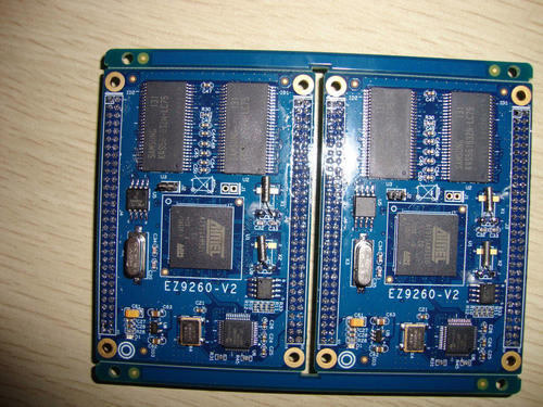
1. Use high-quality raw materials: Choose reliable circuit board suppliers and ensure that the purchased raw materials such as developer and photoresist meet relevant standards and requirements. Under no circumstances should quality be reduced in order to reduce costs. 2. Regular maintenance and update of equipment: Regularly inspect and maintain photosensitive adhesive coating equipment, development equipment, and other related equipment to ensure their normal operation and provide stable performance. 3. Establish a strict quality control process: Develop appropriate quality control and inspection processes to ensure that each production step meets quality standards. Relevant personnel should also receive training to understand and master the correct operating methods. 4. Emphasis on cleanliness and hygiene: Ensure a clean working environment and strictly prohibit pollution sources from entering the production area. Operators should use appropriate protective measures to avoid
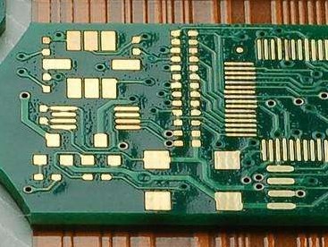
Firstly, it has a high degree of automation and can achieve fully automated bending and bending processes, reducing the possibility of manual intervention and improving production efficiency and quality. Secondly, the mobile FPC bending machine adopts advanced control systems and sensor technology, which can monitor and adjust the bending angle and force in real-time, ensuring that each FPC can meet the design requirements. In addition, the mobile FPC bending machine also has flexibility and adjustability, which can adapt to the bending needs of different models and sizes of FPC. To summarize, mobile phone FPC bending machines play an important role in mobile phone production. It can achieve high-precision bending and bending, improve production efficiency and quality, and has flexibility and adjustability. With the continuous innovation and development of mobile phone exterior design, mobile phone FPC bending machines will continue to play an important role in providing better
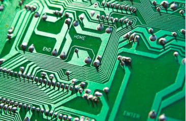
Poor development of PCB circuit boards has always been a common problem faced by manufacturers and the manufacturing industry. With the continuous development and complexity of electronic devices, the requirements for circuit boards have become increasingly high. The problem of unclear development on the circuit board not only affects the quality and performance of the product, but also may lead to functional failure of the product. It is very important to understand the reasons for unclear development and find solutions. 1. Developer contamination: Developer is an indispensable part of the development process of circuit boards, which can remove uncured photosensitive adhesive. However, if the developer is contaminated, such as the presence of precipitates, metal particles, or other impurities, it can lead to unclean development. Solution: Regularly replace the developer and ensure that its quality and purity meet the requirements. At the same time, before using the developer, it
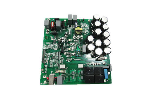
The traditional COF FPC used in the television industry is not much different from ordinary FPC in the production and processing process. In addition to the finer line width and spacing compared to ordinary FPC, FPC is still produced using standard reduction etching method. The COF FPC carrier board used in smartphones is produced using a completely different method from the standard subtractive etching method, using an additive method for semiconductor chips. The industry calls this process the SAP semi additive method. Because the minimum line width and line spacing of FPC produced by standard reduction etching method are generally above 15 microns, it is basically powerless for COF production processes with finer lines. The processing technology of SAP semi additive method mainly comes from SLP type carrier PCB. However, when it entered the smartphone industry, Apple was the first to use this technology on a large scale in the production of mobile phone motherboards. Earlier, w
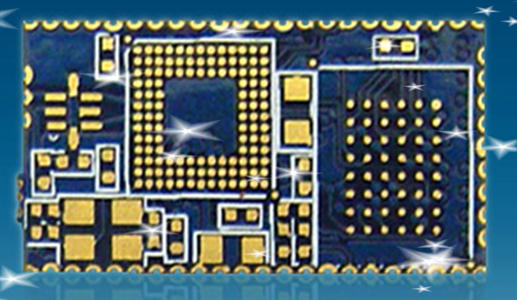
At present, there are approximately 1500 PCB enterprises in China, forming a pattern of joint competition among Taiwanese, Hong Kong, American, Japanese, and domestic enterprises. Among them, foreign-funded enterprises generally have a large investment scale, and have certain advantages in production technology and product specialization; There are many domestic enterprises, but there is still a certain gap in their scale and technological level compared to foreign enterprises. Among them, China's printed circuit industry is mainly distributed in the southeast coastal areas, which is also related to the large demand for water in the PCB industry. These areas are relatively rich in water resources. The Yangtze River Delta and the the Pearl River Delta add up to 90% of the national total. The PCB industry investment analysis indicates that the ratio of the Yangtze River Delta to the Pearl River Delta is about 1:1 at present. The proportion of boards (single panel, double-sided boar
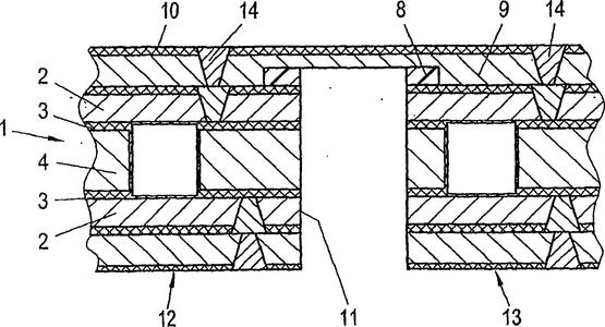
In the era of low profit in electronic products, price wars have changed the supply chain. The total output value of China's PCB industry reached 58.84 billion yuan, an increase of 8.6% year-on-year, with an average compound growth rate of 20% in revenue and a compound growth rate of 27% in net profit attributable to the parent company. The following is an analysis of investment in the PCB industry. Due to the concentration of downstream industries and relatively low labor and land costs, China has become the region with the strongest development momentum. In 2017, China surpassed the United States for the first time and became the world's second largest PCB producer. The proportion of output value also increased from 8.54% in 2000 to 15.30%, nearly doubling. As of 2018, the newly planned investment in China's PCB industry reached 95.5 billion yuan, with 72 new investment projects, with an average investment of 1.3 billion yuan per project. The newly planned investment amounts fo
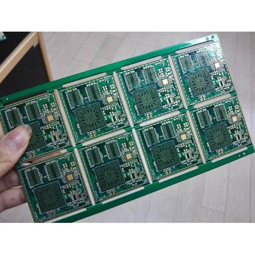
1. Resistor: One of the common components in a circuit. Its main function is to limit the flow of current and control the voltage and current levels in the circuit. By adjusting the circuit signal with different resistance values, it is possible to prevent overcurrent from damaging other components. 2. Capacitor: A common component in a circuit that stores energy. Capacitors can store and release charges under the action of an electric field. It plays a storage and discharge role in the circuit, used for circuit functions such as filtering, coupling, and voltage stabilization. 3. Diode: A nonlinear component in a circuit. Diodes have a single conductivity and can only circulate current in one direction. It is commonly used for circuit rectification, current limiting, and protection functions. 4. Transistor: An important semiconductor device in electronic equipment. The transistor can amplify current and voltage signals, and has various functions such as switching, amplification, a

There are significant differences in usage between rigid circuit boards and flexible circuit boards. Rigid circuit boards are suitable for scenarios with high requirements for stability and reliability, while flexible circuit boards are suitable for scenarios with high requirements for shape and weight. Rigid circuit boards have a fixed shape and size, which can provide good stability and mechanical strength, making them suitable for most general electronic devices. Flexible circuit boards can be bent and folded according to design requirements, with strong shape variability, making them suitable for products with special shapes and lightweight designs. With the continuous development and innovation of electronic products, the application prospects of rigid circuit boards and flexible circuit boards in different fields are becoming increasingly broad. Rigid circuit boards still dominate traditional large electronic devices, but the application of flexible circuit boards in wearabl
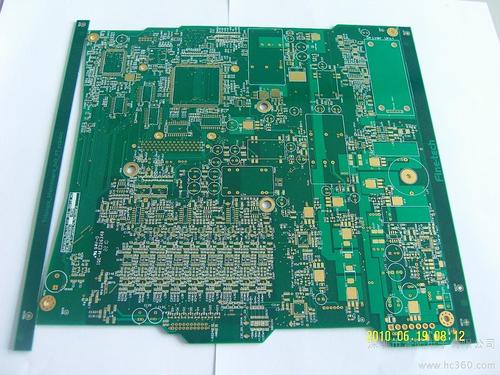
FPC: Flexible Printed Circuit, abbreviated as Flexible Board, in English. It is a single-sided, double-sided, and multi-layer circuit board made by using an etching process on a flexible substrate surface. The surface circuit can also be electrically connected to the inner and outer layers through metallized holes. The production method of flexible circuit boards is simple and cost-effective, while compared to traditional (hard boards), they achieve weight breakthroughs and are thinner. Flexible circuit boards in certain fields can also effectively reduce device volume and facilitate portability. It has a wide range of application scenarios, high experimental value, and long-lasting research and preparation enthusiasm. So far, the vast majority of FPC board circuit fabrication has been done using addition and subtraction (etching) processing, usually by photolithography on copper foil to prepare traditional FPC boards. Firstly, the printing/lithography circuit needs to be printed
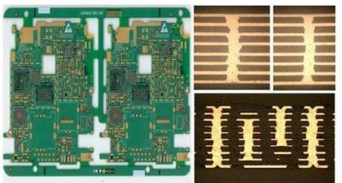
1. One on one assembly board One on one splicing is the simplest splicing method, suitable for small PCB boards with a small quantity. Arrange each small board accurately on the large board according to the design requirements, then perform one-time etching, cutting, and other processes, and finally cut the large board into multiple independent small boards. This method is suitable for sample production or small-scale production, but it is inefficient for large-scale production. 2. Minimize Area Splicing Minimizing area splicing is an optimized splicing method. Arrange multiple small boards on the large board in a certain way to minimize the area of the large board and save materials. This method is suitable for large-scale production, which can improve utilization and reduce costs. 3. Maximize the number of pieces for splicing Maximizing the number of pieces is a splicing method that pursues production efficiency. According to the size and process requirements of the small bo
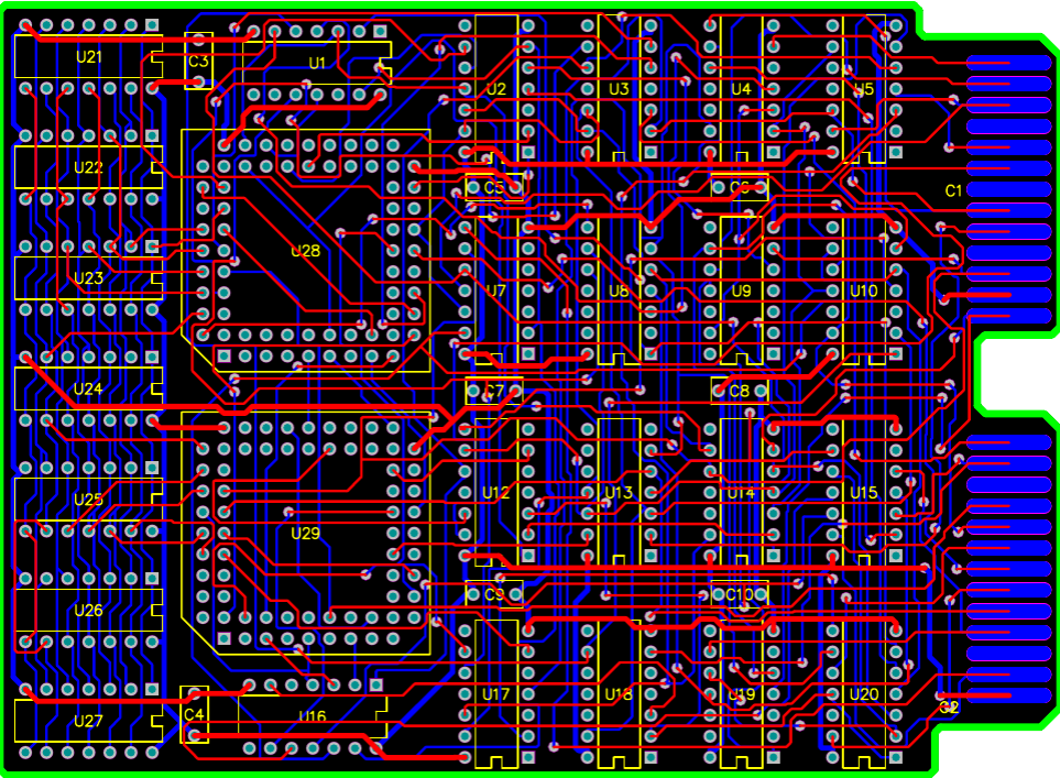
What are the advantages of the product? One is automation. It can be connected to the production line of circuit boards, achieving functions such as automatic feeding, automatic detection, and automatic identification of good and bad products, without the need for manual operation, greatly reducing labor costs and reducing quality damage caused by manual operation. Secondly, high accuracy. Adopting high-precision CIS scanning system, as well as technologies such as automatic positioning, image processing, and intelligent detection and analysis, to achieve high-precision detection. Thirdly, high efficiency. Equipped with a multi-channel detection device, it can customize 3 and 6 channels for simultaneous detection, greatly improving detection efficiency.
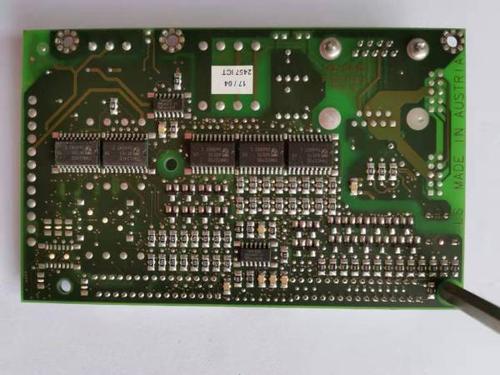
The main problem with RF circuit layout is usually the unsatisfactory characteristic impedance of the circuit, including circuit components and their interconnections. If the copper layer on the lead is relatively thin, it is equivalent to an inductance line and forms a distributed capacitance with other adjacent leads. When the lead passes through a through hole, it also exhibits inductance and capacitance characteristics. The through-hole capacitance mainly comes from the capacitance formed between the copper coating on the through-hole pad side and the copper coating on the formation, which is separated by a relatively small circular ring. Another influence comes from the cylindrical structure of the metal through hole itself. The influence of parasitic capacitance is generally small and usually only causes the edge of high-speed digital signals to deteriorate. The biggest impact of via is the parasitic inductance caused by the corresponding interconnection method. Because in
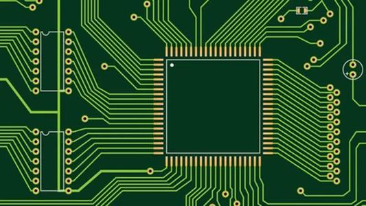
1. High precision: CCD automatic alignment, automatic expansion and contraction to ensure printing accuracy. The maximum printing resolution is 1440dpi. 2. Fine text: Using well-known brand inkjet printing heads for more precise printing quality. Minimum text size 500 μ M/400 μ m. Minimum line width 75 μ M/60 μ M. 3. High efficiency: The multi line inkjet printing head has a higher printing speed. 4. Short cycle: No need to make screen printing, three steps in place, shortening the production cycle. 5. The spray printing area has strong inclusivity: the maximum spray printing area is 610 * 762mm, and the thickness range of the circuit board is 0.1-10mm, with strong inclusivity. 6. Multi spray printing mode: mass production, high-precision, and custom mode. 7. Cost saving: Eliminating various equipment and material costs, as well as labor costs, in the wire mesh process. 8. More environmentally friendly: It does not produce pollutants and is friendly to the environment and op

In recent years, people have increasingly attached importance to environmental protection, so while demanding steady economic development, there are also more requirements for environmental protection construction. Building an "environmentally friendly" society has increasingly become an urgent need for people. The country has also increased its efforts to regulate environmental protection to meet the needs of the times. In 2017, China comprehensively strengthened environmental emission restrictions and conducted inspections on the manufacturing industry, forcing nearly a hundred enterprises to suspend trading for rectification. In 2018, the implementation of the "Environmental Protection Tax" resulted in an increase in environmental protection costs for PCB manufacturers. After a round of rectification, some PCB manufacturers who could not meet environmental requirements were forced to withdraw from the market, and those fortunate enough to survive also had higher requirements fo
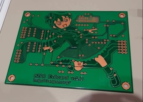
If two holes are too close during drilling operation, it will affect the efficiency of PCB drilling process. Due to the fact that after drilling the first hole, the material in one direction is too thin when drilling the second hole, resulting in uneven stress on the drilling nozzle and uneven heat dissipation of the drilling nozzle, leading to the breakage of the drilling nozzle, resulting in unsightly PCB hole collapse or incomplete drilling. 2. In PC multilayer boards, vias have hole rings on each layer of the circuit, and the environment around each layer of the hole ring varies, with and without wire clips. When optimizing files in PCB factory CAM engineers, they will cut off a portion of the hole ring in cases where the clamping wire is too close or the hole is too close to the hole, to ensure a safe distance of 3mil between the welding ring and different network copper/wire. 3. The hole position tolerance for drilling is ≤ 0.05mm. When the tolerance reaches the upper limit
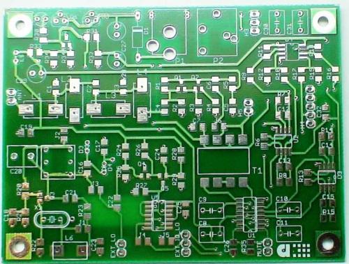
The first level is relatively simple, and the process and process are easy to control. The second order problem starts to get troublesome, one is the alignment problem, and the other is the punching and copper plating problem. There are various second-order designs, one of which is to stagger the positions of each stage and connect the secondary layers through wires in the middle layer, which is equivalent to two first-order HDIs. The second method is to overlap two first order holes and achieve second order through superposition. The processing is also similar to two first order holes, but there are many process points that need to be specially controlled, which is mentioned above. The third method is to directly drill holes from the outer layer to the third layer (or N-2 layer), with many different processes and greater difficulty in drilling. For the third order, the second order analogy is.
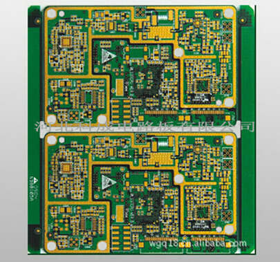
PCB (Printed Circuit Board), also known as Printed Circuit Board in Chinese, is an important electronic component that supports electronic components and serves as the carrier for electrical connections of electronic components. Due to its use of electronic printing technology, it is called a "printed" circuit board. Its main function is to avoid manual wiring errors due to the consistency of similar printed boards in electronic equipment, and to achieve automatic insertion or installation of electronic components, automatic soldering, and automatic detection, ensuring the quality of electronic equipment, improving labor productivity, reducing costs, and facilitating maintenance. HDI boards refer to high-density interconnect circuit boards. The boards with blind hole electroplating and secondary pressing are all HDI boards, which are divided into first, second, third, fourth, and fifth order HDIs. For example, the motherboard of the iPhone 6 is a fifth order HDI. Simply burying

HDI board (High Density Interconnector), also known as high-density interconnect board, is a circuit board that uses micro blind buried hole technology and has a relatively high line distribution density. The HDI board has both inner and outer circuits, which are connected internally by drilling and metallization processes. HDI boards are generally manufactured using the stacking method, and the more times they are stacked, the higher the technical level of the board. Ordinary HDI boards are basically stacked once, while higher-order HDI uses two or more layers of technology, as well as advanced PCB technologies such as hole stacking, electroplating filling, and laser direct drilling. When the density of PCBs increases beyond eight layers, manufacturing with HDI will result in lower costs compared to traditional complex pressing processes. HDI boards are conducive to the use of advanced assembly technology, and their electrical performance and signal accuracy are higher than trad
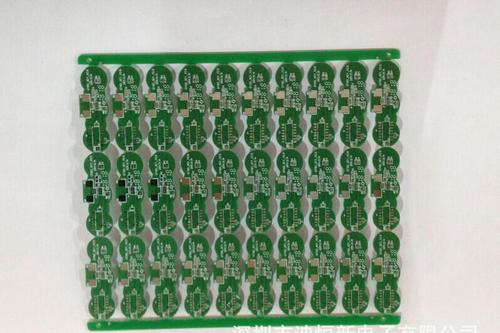
Answer: (1) Solder resist oil is generally composed of a mixture of the main agent, curing agent, and diluent of the ink. During the mixing and stirring of the ink, there will be some air left in the liquid. When the ink is squeezed by a scraper or screen, it flows onto the board surface. In a short period of time, when it encounters strong light or equivalent temperature, the gas inside the ink will flow rapidly with the accelerated flow of the ink, and evaporate outward. (2) The spacing between the lines is too narrow, and the lines are too high. During screen printing, the solder mask ink cannot print onto the substrate, resulting in the presence of air or moisture between the solder mask ink and the substrate. During curing and exposure, the gas expands and causes bubbles due to heat. (3) Single lines are mainly caused by high lines. When the scraper contacts the line, the angle between the scraper and the line increases, making the solder mask ink unable to print to the bottom
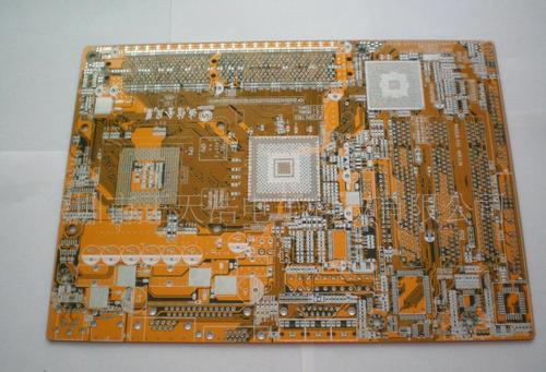
The signal integrity problem is not caused by a single factor, but by multiple factors in board level design. The main signal integrity problems include reflection, ringing, ground bounce, crosstalk, etc. The following mainly introduces the solutions to crosstalk and reflection. Cross talk refers to the unwanted voltage noise interference caused by electromagnetic coupling on adjacent transmission lines when a signal propagates on the transmission line. Excessive crosstalk may cause false triggering of the circuit, resulting in the system not functioning properly. Due to the inverse ratio between crosstalk and line spacing, it is proportional to the parallel length of the lines. Crosstalk varies with the load of the circuit, and for the same topology and wiring situation, the larger the load, the greater the crosstalk. Crosstalk is directly proportional to the signal frequency. In digital circuits, the edge change of the signal has the greatest impact on crosstalk. The faster the
Inquiry Now

