 +86 755 2794 4155
  sales@knownpcb.com
-
Shenzhen KNOWNPCB Technology Co., Ltd.
 +86 755 2794 4155
  sales@knownpcb.com
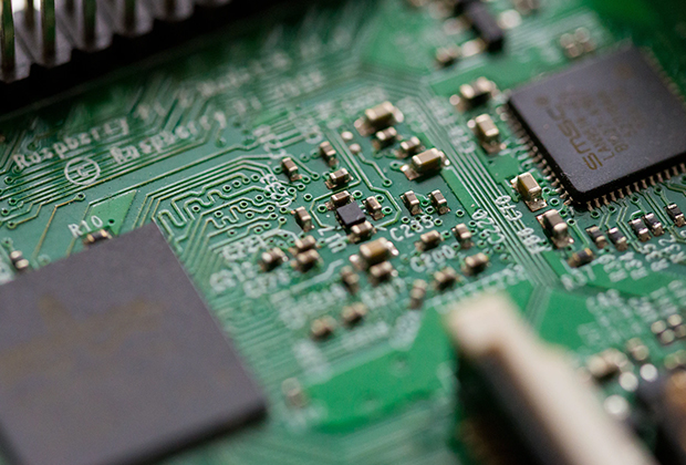
Have you noticed that now more and more of our lighting is using led lighting.What is LED? Compared to the traditional light bulbs, LEDs have lower power consumption, longer lifetime and higher energy efficiency. In the PCB industry,when we say LED PCB, it refers to the pcb used for LED lighting, if you are looking for a suitable LED PCB for your lighting system, this article may bring you something. WHAT ARE LEDS COMPOSED OF?LED is an initial light-emitting diode that produces light when an electric current passes through. LEDs typically have negative and positive electrodes, which generate light in the visible light region.The LEDS are glued to the PCB by soldering process and have electrical connections for lighting.Since light-emitting diodes dissipate a lot of heat when they are in use, when you are designing LED, the metal core is usually the best choice for LED PCB, it is because that it dissipates heat more faster. Among them, the metal material aluminum is the most widely used
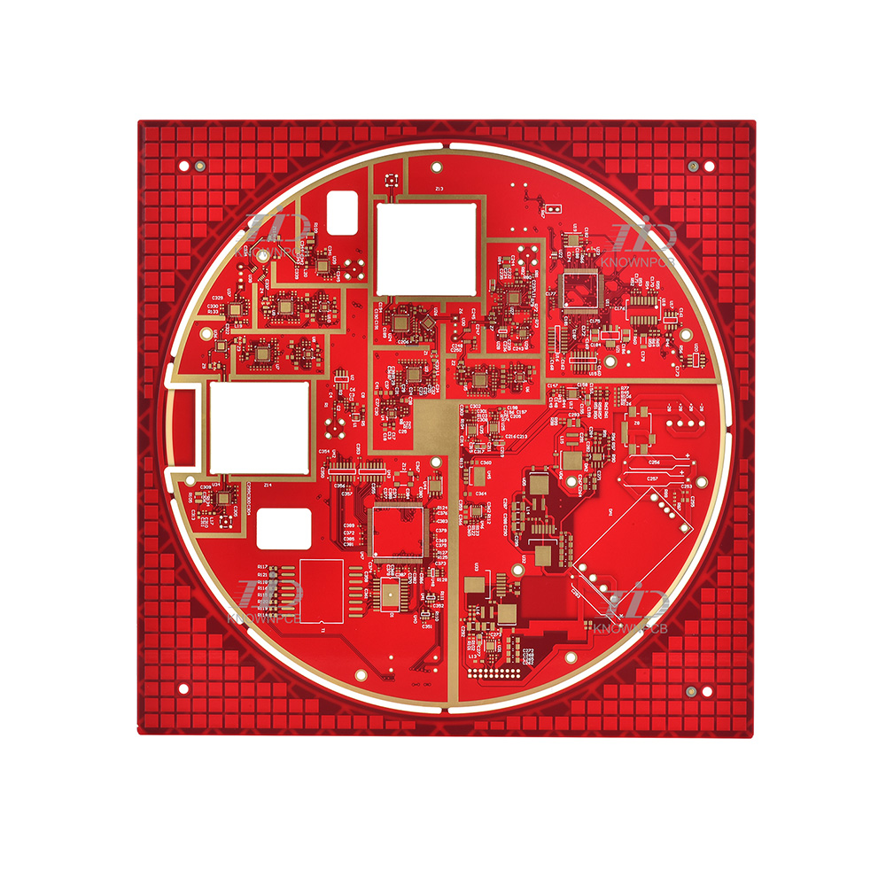
In wave soldering, the main process materials used are flux and solder. 1. The application of flux can remove oxides from the welding surface, prevent reoxidation of the solder and welding surface during welding, reduce the surface tension of the solder, and help transfer heat to the welding area. Flux plays a crucial role in controlling welding quality. At present, the most commonly used flux for wave soldering is non cleaning flux, and there are the following requirements when selecting flux: (1) The melting point is lower than that of solder; (2) The infiltration diffusion speed is faster than that of melted solder; (3) The viscosity and specific gravity are smaller than those of solder; (4) Stable storage at room temperature. 2. Quality control of solder Tin lead solder continuously oxidizes at high temperatures (250 ℃), causing a continuous decrease in the tin content of the tin lead solder in the tin pot, deviating from the eutectic point, resulting in poor flowability
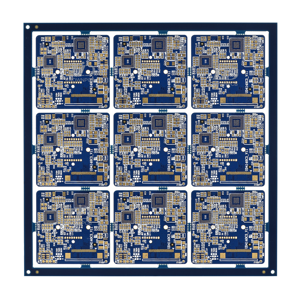
1. Pad design (1) When designing plug-in component pads, the pad size should be designed appropriately. If the solder pad is too large, the solder spreading area is large, and the formed solder joints are not full, while the surface tension of the smaller solder pad copper foil is too small, and the formed solder joints are non wetting solder joints. The fit gap between the aperture and the component lead is too large, which is prone to false soldering. When the aperture is 0.05-0.2mm wider than the lead and the diameter of the solder pad is 2-2.5 times the aperture, it is an ideal welding condition. (2) When designing solder pads for SMD components, the following points should be considered: in order to eliminate the "shadow effect" as much as possible, the solder end or pin of SMD should be facing the direction of the tin flow to facilitate contact with the tin flow and reduce false soldering and solder leakage. For smaller components, they should not be placed behind larger co
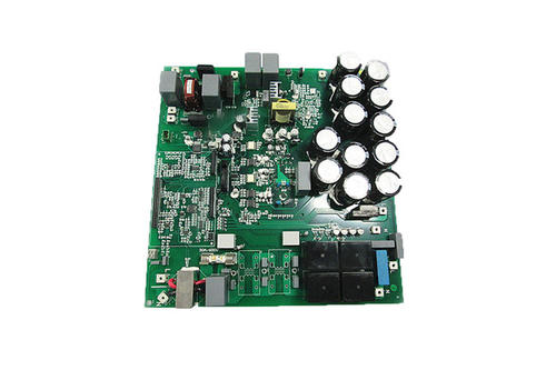
In recent years, with the continuous development of electronic products and the further advancement of intelligence, the design of printed circuit boards (PCBs) has become increasingly important. The design of PCB multilayer structure occupies a core position in modern electronic equipment, and its rationality directly affects the performance and reliability of electronic products. Firstly, let's take a look at the design principles of a multi layer PCB structure. Firstly, the selection of layers is very important. The more layers there are, the higher the complexity of signal transmission, so a balance between circuit complexity, electromagnetic interference, and cost needs to be considered in the design. Secondly, in the design of PCB multilayer boards, the signal circuits of each layer should be reasonably arranged. There should be sufficient spacing between different signal lines to avoid mutual interference. In order to improve the speed of signal transmission and reduce ele
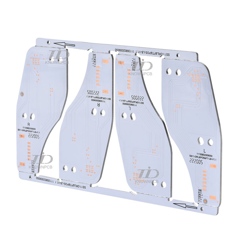
With the continuous development of technology, LED circuit boards are playing an increasingly important role in the lighting industry. They not only provide high brightness lighting effects, but also have advantages such as energy conservation, environmental protection, and long service life. In order to further promote the development of LED light circuit boards, new design trends are constantly emerging. Today, the editor will delve into the current 5 cutting-edge LED light board PCB design trends and look forward to the possibilities that technology can bring to the future. Firstly, customized design has become mainstream. Traditionally, the design of LED light circuit boards has been relatively uniform, but now the market demand is constantly personalized, and people's requirements for lighting are becoming increasingly diverse. Therefore, more and more lamp panel manufacturers are providing customized design services to meet the needs of different customers. Customized desig
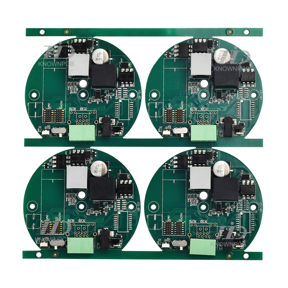
Firstly, the first step in the production of new energy vehicle PCB boards is the design of circuit board drawings. The designer draws the layout and circuit connection drawings of the circuit board based on the functional and dimensional requirements of the electronic equipment of the new energy vehicle. The accuracy and rationality of design drawings are crucial for the subsequent manufacturing process. Next is the plate making and electroplating of the circuit board. Plate making is the process of transferring design drawings to photoresist through lithography technology, and then gradually exposing the copper layer through chemical corrosion to form the required circuit lines. Next, the copper plate is immersed in an electroplating bath, and through the action of current, a layer of copper foil is formed on the circuit line to enhance conductivity and durability. The third key step is drilling and deburring. In this step, the high-speed drilling on the small lathe drills n

1. Design and Planning: Based on the functions and requirements of the sensor, the manufacturer designs and plans to determine the required type and size of the circuit board. 2. Material selection: According to design requirements, select suitable circuit board materials, usually using FR-4 glass fiber composite material. 3. Printed Circuit Board (PCB) Manufacturing: Using printing technology to create circuit patterns on a substrate. This process involves processing the copper foil layer into the desired circuit shape, covering the surface of the circuit board with photosensitive adhesive, and using ultraviolet radiation to define the circuit pattern. 4. Chemical etching: By chemical etching, unnecessary copper foil layers are peeled off, leaving only the required wiring. This ensures that the circuit will not short-circuit. 5. Punching: Drill holes in the locations where components need to be installed to facilitate the installation of electronic components. 6. Assembly of
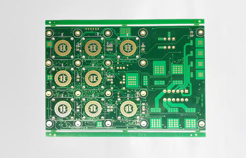
Industrial circuit board damage usually refers to a component being damaged, possibly a chip, a capacitor, or even a small resistor. The repair process involves identifying and replacing the damaged component. 1. Resistors with small resistance values and capacitors with large capacity are prone to damage A resistor with a small resistance value is often used in power supply lines to limit current, which acts as a fuse. If the current is too high, it will first burn out. In addition, many ground capacitors are used in power supply lines for filtering, and their size and capacity are generally large. If the voltage or current is unstable, the capacitors will break down and cause leakage. 2. Fault characteristics and maintenance of capacitor damage The failure caused by capacitor damage is the highest in electronic devices, with electrolytic capacitor damage being the most common. Capacitor damage is manifested as: 1. reduced capacity; 2. Complete loss of capacity; 3. Leakage; 4

(1) There should be a reasonable direction: such as input/output, AC/DC, strong/weak signals, high-frequency/low-frequency, high-voltage/low-voltage, etc. Their direction should be linear (or separated) and should not blend with each other. Its purpose is to prevent mutual interference. (2) Choose a good grounding point: For example, the multiple ground wires of the forward amplifier should be merged before connecting to the main ground, etc. (3) Reasonably arrange the power filter/decoupling capacitors: Generally, only a few power filter/decoupling capacitors are drawn in the schematic diagram, but they are not indicated where they should be connected. In fact, these capacitors are designed for switching devices or other components that require filtering/decoupling, and they should be arranged as close to these components as possible. (4) There is a particular emphasis on lines: if conditions permit, lines that are wide will never be thin; High voltage and high-frequency lines
The through hole plays a role in connecting and conducting circuits, and the development of the electronics industry has promoted the development of PCBs, resulting in the emergence of plug hole technology. In order to meet the customer's requirements, the process of conducting and plugging holes can be described as diverse, with a particularly long process flow and difficult process control. So, how is the process of plugging through holes in PCB circuit boards achieved? Let's take a look together with the editor: 1、 Plug hole process after hot air leveling This process flow is: board surface resistance welding → HAL → plug hole → curing. Production is carried out using a non plug hole process, and after hot air leveling, aluminum mesh plates or ink blocking nets are used to complete the plug holes of all fortresses. Plug ink can be used as photosensitive ink or thermosetting ink. This process flow can ensure that the guide hole does not fall off oil after hot air leveling, but
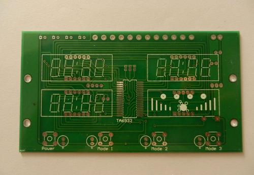
What are the design requirements for PCB printed circuit boards in PCB sampling? Let's take a look together: 1. Accurate This is the most basic and important requirement for printed circuit board design. Accurately implement the connection relationship of the electrical schematic diagram to avoid errors such as "short circuit" and "open circuit". Generally, products need to undergo more than two rounds of trial production and modification, while CAD software with strong functions has inspection functions to ensure the correctness of electrical connections. 2. Reliable A correctly connected circuit board may not necessarily have good reliability, such as improper selection of boards, incorrect board thickness and installation fixation, improper component layout and wiring, etc., which may cause the PCB to not work reliably. 3. Reasonable A printed circuit board component is closely related to the rationality of the printed circuit board, from manufacturing, inspection, assembl
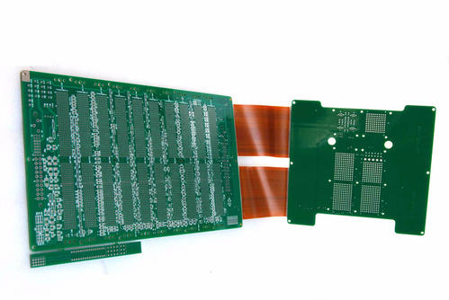
A rigid circuit board is a type of circuit board with a fixed shape and size, usually made of glass fiber cloth based (FR-4) material. Due to its high strength and good electrical performance, rigid circuit boards are widely used in scenarios that require high stability and reliability, such as motherboards for electronic products such as computers, mobile phones, televisions, etc. Rigid circuit boards have good mechanical strength and can fix various electronic components, ensuring the stability and reliability of the circuit. The advantages of rigid circuit boards are high stability and low cost, which are suitable for most general electronic devices. Its rigid structure can provide good resistance to vibration and impact, which helps improve the stability and reliability of electronic products in use. In addition, the manufacturing process of rigid circuit boards is mature, with relatively low costs, suitable for large-scale production, and is also a mainstream choice in the fiel
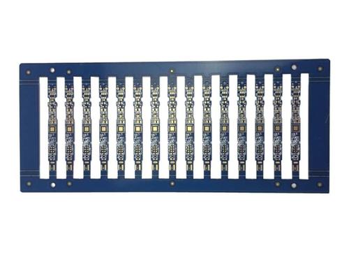
The development of future automotive circuit boards can foresee two major trends: intelligence and environmental protection. Intelligence is because, with the development of technology, cars are increasingly relying on electronic technology, especially the application of AI artificial intelligence technology, which greatly improves the intelligence of car circuit boards and endows cars with more possibilities. Environmental protection is due to the production of harmful substances such as copper, nickel, lead, and other heavy metals during the manufacturing process of circuit boards, which pollute the environment after being discarded. Therefore, environmentally friendly design and manufacturing, as well as the recycling of circuit boards, will be an important trend for future development. The importance of automotive circuit boards as the brain of automobiles is self-evident. Whether it is the daily operation of cars or bringing humanized intelligent driving to cars, it is insep
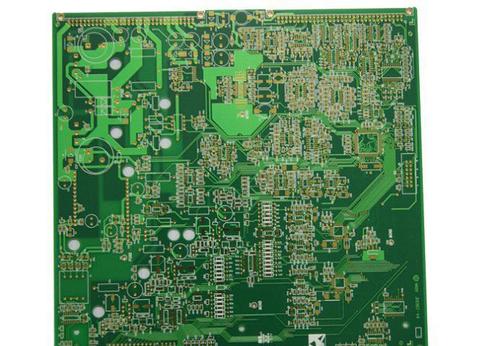
A car circuit board is like the brain of a car, which can accurately control various functions and performance of the car. It is connected to the engine, battery, brake, navigation, audio, lighting, and other components of the car to transmit and interact information, quickly respond to the driver's operating instructions, and then control the car's movement. In addition to being able to connect various components of the car, the circuit board of Yinmei Automobile also has some special functions. For example, a large number of intelligent sensors on modern car circuit boards can monitor the working status of the car in real-time, including engine temperature, throttle opening, brake pressure, etc. These data will be fed back to the driver in real-time, allowing the driver to have a clearer understanding of various information about the car. In addition, car circuit boards can also achieve some special functions, such as autonomous driving, adaptive cruise control, automatic parki
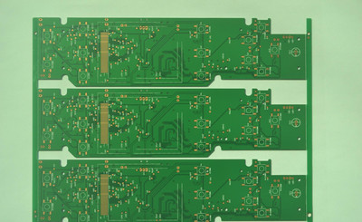
The production process of automotive circuit boards involves numerous materials and processes, requiring rigorous design and precise manufacturing. Firstly, the designer will design a circuit diagram that meets the performance and control requirements of the car. Then, the circuit diagram will be converted into a physical circuit board substrate, which requires the use of a high-precision exposure technology called "light drawing". Next, the circuit board substrate will undergo copper plating treatment to form a conductive circuit path. Then, various electronic components such as capacitors, resistors, diodes, transistors, etc. will be soldered onto the channel. Finally, these circuit boards will be tested and debugged to ensure that their performance meets the actual usage needs of the car. The maintenance and upkeep of car circuit boards is very important, otherwise it may affect the normal operation of the car and even cause malfunctions. Firstly, users should avoid using cars
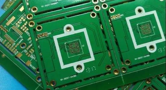
Firstly, white oil can provide good insulation protection. In electronic devices, PCB boards carry numerous electronic components, which often require a certain degree of electrical isolation between them. The coating of white oil can form a layer of insulation protection film, effectively isolating the electrical connection between components and avoiding the occurrence of circuit short circuits and other problems. Secondly, white oil can prevent oxidation and corrosion. The surface of PCB boards is easily affected by oxidation when exposed to air, leading to the loss of conductivity of metal materials and even damage to circuits. The coating of white oil can form a protective layer that isolates air from direct contact with the PCB board, effectively preventing oxidation and corrosion, and extending the service life of electronic devices. In addition, white oil also has the function of dust and moisture prevention. In practical applications, PCB boards are often affected by ex
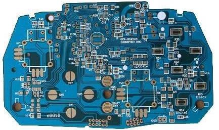
For circuit board design, shape is very important as it directly affects the performance and reliability of the circuit. Let's take a look at the manufacturers of intelligent circuit boards together! A suitable exterior design can improve the manufacturing efficiency and installation convenience of circuit boards. When choosing the appearance, we should follow the following principles: 1. Simplicity and clarity: The appearance of a PCB circuit board should be concise and clear, without excessive curves or patterns. This helps to control the manufacturing process and reduce manufacturing costs. 2. Reasonable use of space: According to actual needs, make reasonable use of the space on PCB circuit boards to avoid waste. At the same time, it is necessary to consider whether the size of the board is suitable for installation in the target device. 3. Consider edge treatment: When designing the shape of a PCB circuit board, the method of edge treatment should be considered. You can ch
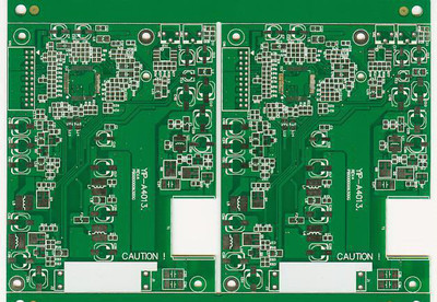
Question 1: How to solve the inconsistency between the circuit schematic and the board copying result? To address this issue, we need to start from the source. Firstly, ensure the accuracy of the circuit schematic to avoid errors or omissions. Secondly, check the correspondence between the schematic diagram and the copied board file to ensure that there is no confusion or misalignment. Finally, professional schematic comparison tools can be used to check layer by layer and eliminate possible problems. Question 2: How to solve the problem of component loss or misalignment during the copying process? Component loss or misalignment is a common problem, but it can also be prevented and resolved. Firstly, it is recommended to prepare a component list and check the position and number of each component before copying to avoid omissions. Secondly, leave sufficient space during wiring to avoid interference and misalignment between components. Finally, during the placement process, stric
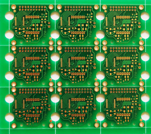
With the development of modern technology, the electronic products around us have become increasingly intelligent and precise. As the core of these electronic products, the importance of printed circuit boards (PCBs) has also become increasingly prominent. So, have you ever been curious about what PCB sampling is? How does it play a crucial role in product development? Intelligent circuit board manufacturers will reveal this knowledge and popular science topic for you. PCB sampling, in simple terms, is to verify the correctness, stability, and feasibility of circuit design by producing a small number of sample circuit boards. It is one of the indispensable links in the product development process Why do we need to conduct PCB sampling? There are three reasons: Firstly, PCB sampling can help developers discover and solve problems in circuit design in a timely manner. In the product design phase, especially for complex circuit designs, it is difficult to completely avoid errors o

The full name of FPC is Flexible Printed Circuit, which is a flexible printed circuit board. Unlike traditional hard circuit boards, FPC is made of flexible materials with characteristics such as bending, folding, and bending. It can better adapt to the curved design of mobile phones, providing higher reliability and stability. The FPC bending machine for mobile phones plays an important role in the production of mobile phones. It is mainly used for precise bending and bending of FPC to meet the requirements of mobile phone appearance design. Innovative designs such as curved screens and foldable screens in mobile phones cannot do without the support of the FPC bending machine. The function of mobile FPC bending machine is mainly reflected in the following aspects. Firstly, it can achieve high-precision bending and bending, ensuring the accuracy and stability of FPC during the phone assembly process. Secondly, mobile phone FPC bending machines can improve production efficiency
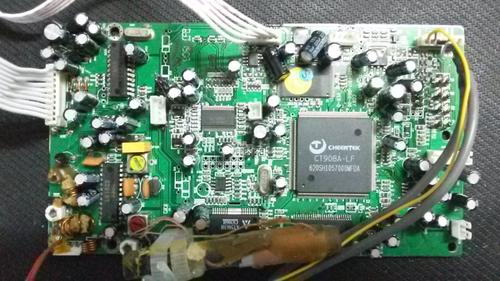
The types of FPC board substrates mainly include polyimide (PI), polyamide acid (PAA), polyamide ester (PA), polyaniline ester (PEN), and fluoroplastics (FEP). Polyimide is the most common substrate with good heat resistance, chemical corrosion resistance, and mechanical properties, suitable for high-temperature and high-frequency applications. PAA substrates are relatively inexpensive, but have poor heat and chemical resistance, making them suitable for low-cost and general performance requirements applications. PA and PEN substrates are intermediate in terms of heat resistance, chemical resistance, and mechanical properties between polyimide and PAA, making them suitable for various moderately demanding applications. The characteristic of FEP substrate is its excellent flame retardancy and electrical properties, suitable for high demand applications. When selecting FPC board substrate, it needs to be determined based on specific application requirements and performance requirem
Inquiry Now

