 +86 755 2794 4155
  sales@knownpcb.com
-
Shenzhen KNOWNPCB Technology Co., Ltd.
 +86 755 2794 4155
  sales@knownpcb.com
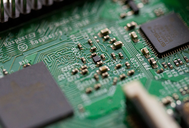
Have you noticed that now more and more of our lighting is using led lighting.What is LED? Compared to the traditional light bulbs, LEDs have lower power consumption, longer lifetime and higher energy efficiency. In the PCB industry,when we say LED PCB, it refers to the pcb used for LED lighting, if you are looking for a suitable LED PCB for your lighting system, this article may bring you something. WHAT ARE LEDS COMPOSED OF?LED is an initial light-emitting diode that produces light when an electric current passes through. LEDs typically have negative and positive electrodes, which generate light in the visible light region.The LEDS are glued to the PCB by soldering process and have electrical connections for lighting.Since light-emitting diodes dissipate a lot of heat when they are in use, when you are designing LED, the metal core is usually the best choice for LED PCB, it is because that it dissipates heat more faster. Among them, the metal material aluminum is the most widely used
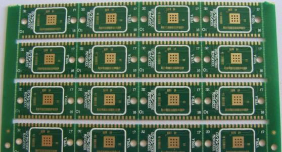
First, it is equal length. When designing a differential line, pay attention to making the lengths of the two signal lines the same. Because the length of the signal lines is the same, the transmission time of the signals is also the same, so the polarities of the differential signals will be different, resulting in the opposite situation. If the differential signal is the same, the signal quality will be poor.Next, is the isometric. That is to say, the distance between pairs of differential lines should be consistent. By adjusting the distance of the differential line, we can adjust a differential impedance in the whole process. What is the benefit of doing this? If our differential impedance can maintain a certain continuity, then there will be very few reflections and the transmitted signal will be very complete.Finally, it is the stacking of differential lines and printed boards. It is generally believed that the differential line will provide a reflow path for the printed board, a
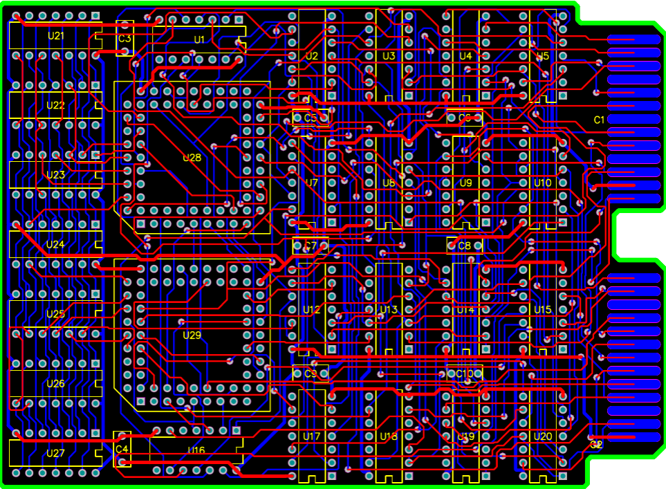
First, it is equal length. When designing a differential line, pay attention to making the lengths of the two signal lines the same. Because the length of the signal lines is the same, the transmission time of the signals is also the same, so the polarities of the differential signals will be different, resulting in the opposite situation. If the differential signal is the same, the signal quality will be poor. Next, is the isometric. That is to say, the distance between pairs of differential lines should be consistent. By adjusting the distance of the differential line, we can adjust a differential impedance in the whole process. What is the benefit of doing this? If our differential impedance can maintain a certain continuity, then there will be very few reflections and the transmitted signal will be very complete. Finally, it is the stacking of differential lines and printed boards. It is generally believed that the differential line will provide a reflow path for the printed
1. Report the results of the work The leader who lifts the heavy weight is the favorite. When reporting work, please remember to report the result to the leader first, and the result thinking is the first thinking. 2. Ask for work plan Please ensure that at least two programs are given to leaders, and express their views and effective suggestions. Don't let the leader do the quiz questions, but let the leader do the multiple-choice questions. Don't ask the leader how to do this thing, what to do, but ask, I have a plan, you can listen to it and see how it goes! 3. Summarize the work process and find three points To do a work summary, it is necessary to describe the process, not only to have a clear sequence and logic, but also to find out the key points, mistakes, and reflection points in the process. 4. Arrange work standards and clarify customer requirements Layout work must be clear about customer requirements and quality standards, otherwise subordinates will not know ho
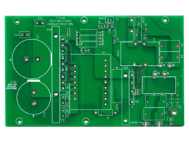
After the customer's plug-in test, it is found that the via hole (via hole) is not connected. The test can be carried out normally before the plug-in, and the appearance has no drilling deviation phenomenon, which is mainly caused by the following five reasons: First: the hole copper is not enough; Second: the roughness of the hole wall is too large Third: Drilling dust plug holes Fourth: drilling broken knife to make up holes Fifth: poor solder mask plug hole In terms of controlling the problem of through-hole failure, the hole copper is the most important link. The automatic sinking copper line of our Honglian circuit is not small: Detection: The detection method of immersion copper wire is mainly backlight series detection. The number of series is more than 9 to be qualified to ensure the quality of copper immersion and hole formation. The detection methods include deposition speed force detection (copper layer thickness in standard time); glue removal speed force (this

One, circuit board factory tin surface quality defects So what are the factors that cause the bad tin surface of the tin surface? According to the analysis of the editor, there are the following points 1. The operation is not in accordance with the operating specifications when shipping The circuit industry has extremely strict requirements on the workshop environment and the standard operation of employees, especially the chemical reaction environment is required in the circuit board production process, so the infiltration of impurities is not allowed. After the board spraying process is completed, the subsequent one All series require employees to wear anti-static gloves to operate, because finger sweat or stains directly contact the surface, which will cause surface oxidation. If it causes defects, it is extremely difficult to find, and it is irregular, and it is difficult to be exposed in testing and tinning experiments. 2. The tin furnace for spraying tin is not cleaned on
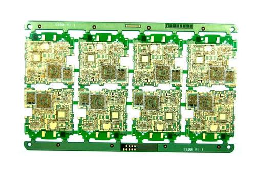
1. Report the results of the work The leader who lifts the heavy weight is the favorite. When reporting work, please remember to report the result to the leader first, and the result thinking is the first thinking. 2. Ask for work plan Please ensure that at least two programs are given to leaders, and express their views and effective suggestions. Don't let the leader do the quiz questions, but let the leader do the multiple-choice questions. Don't ask the leader how to do this thing, what to do, but ask, I have a plan, you can listen to it and see how it goes! 3. Summarize the work process and find three points To do a work summary, it is necessary to describe the process, not only to have a clear sequence and logic, but also to find out the key points, mistakes, and reflection points in the process. 4. Arrange work standards and clarify customer requirements Layout work must be clear about customer requirements and quality standards, otherwise subordinates will not know ho
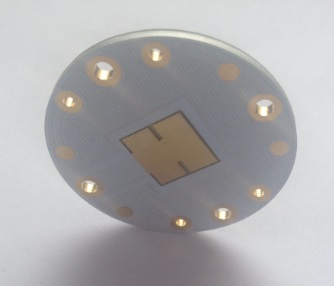
1. Temperature of soldering iron SMT tends to work at a temperature equivalent to that of a hot soldering iron (approximately 375 ℃), making things faster and requiring fine-grained IC welding techniques to work below. The actual temperature setting will vary for different irons, but it may range from 330 ° C/626 ° F to 380 ° C/716 ° F (although some inexpensive temperature controlled soldering irons may not have accurate temperature settings if they do not work well, so try to be higher). Most modern components have a considerable amount of elasticity and are designed to handle automatic welding and lead-free solder, but even at these high temperatures, it is best not to leave contact with the iron for too long, 2. Solder 0805 chip resistors and capacitors Apply flux to both pads. Use tweezers and/or tips to achieve the position of the component. Load some solder onto the soldering iron head. At the same time, use a tip to keep the component in place, and touch the soldering
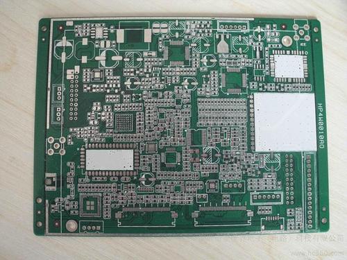
As a provider of electrical connections for electronic components, PCB is known as the "mother of electronic products". It is understood that each electronic product requires customized circuit boards, which means that no matter how the electronic industry's products are upgraded, there will be a continuous demand for circuit board copying. In addition to imitating and cloning existing circuit boards, PCB copying can also improve existing technology and accelerate the upgrading and upgrading of electronic products. Therefore, we can also say that the PCB copying industry is a very active industry in the electronic component industry. From the perspective of industry division, PCB copying is undoubtedly a segmented and special industry, and its industry characteristics determine that PCB copying enterprises have their own business characteristics. Currently, with electronic component products becoming increasingly miniaturized and complex, global PCB copying manufacturers are facing
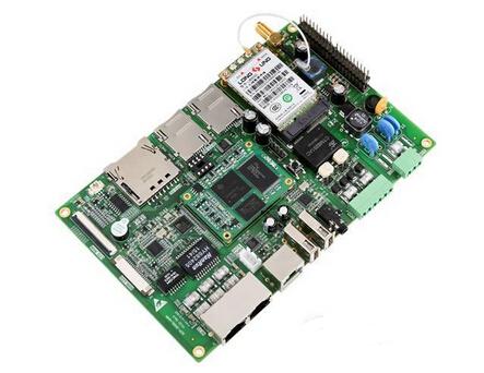
1: Establish encapsulation that is not present in the encapsulation library. Before designing the PCB board sample diagram, if a certain component in the schematic diagram cannot find a packaging model in the packaging library, it is necessary to use the component packaging model editor to create a new one. It is necessary to ensure that the packaging model of the used component is complete in the packaging library (which can be multiple library files) to ensure the smooth progress of PCB design. 2: Set PCB board design parameters. According to the needs of circuit system design, set the number of layers, size, color, etc. of the PCB board. 3: Load network table. Load the network table generated from the schematic diagram and automatically load the component packaging model into the PCB design window. 4: Layout. A combination of automatic and manual layout methods can be used to place the component packaging model in an appropriate position within the PCB planning range, making
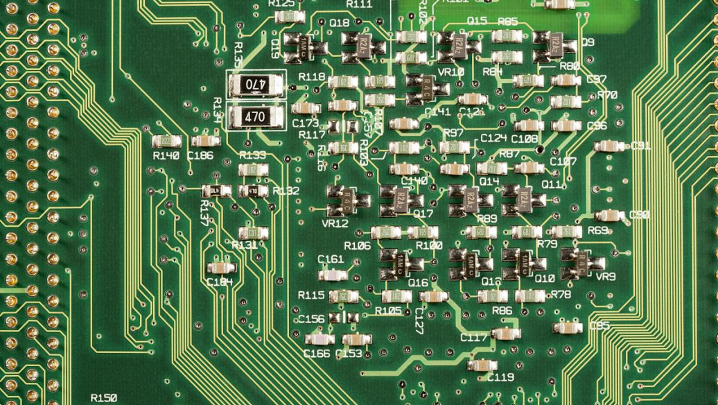
1: The distance from the edge of the circuit board is generally not less than 2MM. The shape of the circuit board is rectangular, and the aspect ratio is 3:2 or 4:3. When the surface size of the circuit board is greater than 200MM by 150MM, the mechanical strength that the circuit board can withstand should be considered. 2: In general, all components should be arranged on the same side of the circuit board. Only when the top layer components are too dense can some highly limited and low heat generating devices, such as SMD resistors, capacitors, ICs, etc., be placed on the lower layer. 3: The minimum spacing between adjacent solder pads of different components on the PCB sample circuit board should be at least 1MM. 4: On the premise of ensuring electrical performance, components should be placed on a grid and arranged parallel or perpendicular to each other, in order to be neat and beautiful. In general, components are not allowed to overlap; The arrangement of components shoul
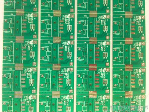
Counting the busy people in 2012, there are indeed many. Du Fu is busy getting graffiti, Mr. Bao is busy clarifying his skin color, and Yuan Fang is busy answering questions and solving doubts. However, the busiest thing to say is the consumers who choose from countless electronic products. The electronics industry is fiercely competitive, and consumers are undoubtedly the biggest beneficiaries. Under the competition of electronic products, the electronic component industry has attracted much attention. When PCB copying breaks the traditional circuit board industry and embarks on a "non mainstream" path, colorful and exciting scenes will surely unfold one after another. Circuit boards are important electronic components and support electronic components. Circuit board copying (PCB copying) is a reverse research technique that can visualize the core technology of electronic products and absorb it into one's own technology. As a leading enterprise in the board copying industry, Xing
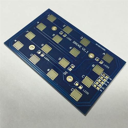
1. Function and Characteristics: Nickel plating is used as a substrate coating for precious and base metals on printed circuit boards (PCB), and is also commonly used as a surface layer for certain single-sided printed boards. The PCB sampling manufacturer tells you that for heavy load worn surfaces such as switch contacts, contact pads, or plug gold, using nickel as the gold substrate coating can greatly improve wear resistance. When used as a barrier layer, nickel can effectively prevent the diffusion between copper and other metals. The combination coating of matte nickel/gold is often used as a metal coating for corrosion resistance, and can meet the requirements of hot pressing welding and brazing. Only nickel can be used as a corrosion resistant coating with ammonia based etchants, and PCBs that do not require hot pressing welding and require a bright coating are usually coated with smooth nickel/gold. The thickness of nickel coating is generally not less than 2.5 microns, us
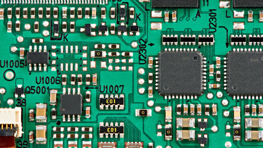
1. During the production process, loose materials may be generated due to equipment and other factors. Therefore, during the operation process, the operator should check the material step distance before pasting and when taking over the shift. Each time the garbage is poured, the throwing box and garbage bin should be checked to collect the loose materials. At the same time, excessive abnormal situations of loose materials should be reported to the line leader. 2. Classify the bulk materials according to the appearance of the components, and verify the back pattern of the components to determine the material code. Then, package the verified bulk materials in an anti-static bulk box or bag, and mark the material code with the signature of the confirming person. 3. The loose materials generated on duty should be loaded 1 hour before work or when there are still 100 pieces left on the task order. When the loose materials are online, the operator first checks the material code and ba
First of all, let's talk about the difference: through holes are drilled holes on PCBs, usually used for interlayer conductivity and also for heat dissipation. A pad is a pad on a via, just like a pad for inserting devices. But! In the production and manufacturing process of PCB circuit boards, their processing methods are different. 1. The number of holes indicated in the design of VIA is determined by drilling. Then there are also process steps such as copper deposition, and the actual pore size will be approximately 0.1mm smaller than the designed pore size. For example, if the through-hole is set to 0.5mm, the actual aperture after completion is only 0.4mm. 2. The aperture of PAD will increase by 0.15mm during drilling. After undergoing copper deposition process, the aperture is slightly larger than the designed aperture, about 0.05mm. For example, if the designed aperture is 0.5mm, the drilling will be 0.65mm, and the completed aperture will be 0.55mm. 3. VIA may be co
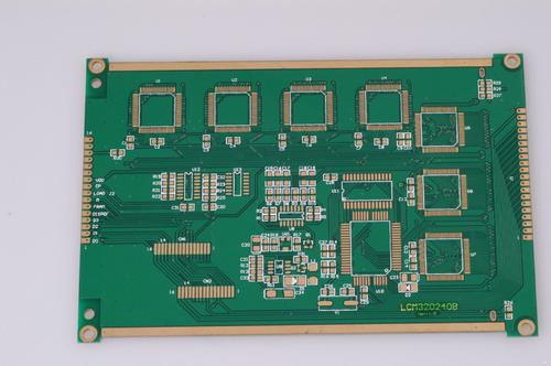
SMT processing is the most common technology in the SMT processing industry. What questions do we need to know about such a process? How can we comprehensively understand the technology of SMT processing? How can we comprehensively understand the factors that contribute to these problems? Here are a few points for you: 1: Placement of SMT processing: Its function is to accurately install surface mounted components onto the fixed position of the PCB. The equipment used is a placement machine, located behind the screen printing machine in the SMT production line. 2: Screen printing for SMT processing: Its function is to leak solder paste or SMT adhesive onto the PCB pad, preparing for the welding of components. The equipment used is a screen printing machine (screen printing machine), located at the forefront of the SMT production line. 3: Solidification of SMD processing: Its function is to melt the SMD adhesive, thereby firmly bonding the surface assembled components with the PC
The current management situation of small and medium-sized enterprises in China can be divided into three types: first, management without management; Secondly, there is management, but the form of expression is relatively extensive; The third is to have management, but it is not the crystallization of the natural development of one's own enterprise, but rather a product that is "borrowed" and basically belongs to the type of "copying and copying". 1. There is no "management" management, which means that enterprises do not have a fixed management model and rely solely on command and command to act. In this type of enterprise, there is no organizational structure, no clear division of labor, and often an employee has to hold multiple positions, with the element of human governance running through it. The management of the enterprise relies entirely on the consciousness of family relationships, and commands or commands fill the entire process of enterprise management. Usually, there
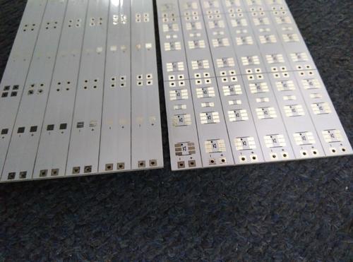
The exceptionally weak quality control and technical management in circuit board factories can lead to product quality problems. The quality department and technical department are important in circuit board enterprises, and most circuit board factories with abnormal quality have a common point, which is chaotic internal management. So, in order to improve product quality and reduce manufacturing costs, the circuit board sampling manufacturer tells you that the circuit board factory should have made improvements in the following aspects: 1. Everyone has responsibilities and everything has a process The circuit board factory should clarify the functions and job responsibilities of the technical and quality departments, especially for order review, product process drawings, FPC/PCB inspection standards, etc., to avoid the production and material departments from privately changing information. The biggest taboo in management is to rely on power for management. Circuit board factories
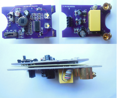
1、 PCB copying material Taking ordinary double-sided sheet metal as an example, sheet materials generally include FR-4, CEM-3, etc., with sheet thicknesses ranging from 0.6mm to 3.0mm, and copper thicknesses ranging from frac12oz to 3oz, all of which cause significant price differences in sheet metal; In terms of solder resist ink, there is also a certain price difference between ordinary thermosetting oil and photosensitive green oil. 2、 PCB board copying production process Different production processes can result in different costs, such as gilded and tinned plates, gongs (milled) and beers (punched) plates for manufacturing shapes, and the use of silk screen and dry film circuits. 3、 PCB copying difficulty Even if the materials and processes are the same, the difficulty of the PCB itself will result in different costs. If there are 1000 holes on both types of circuit boards, and one board has a hole diameter greater than 0.6mm and the other board has a hole diameter less t
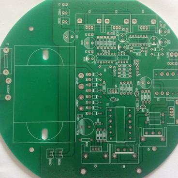
In recent years, Pcb liquid medicine has gradually shifted from being environmentally friendly to being environmentally friendly. The government has increased its punishment efforts, and the industry and PCB manufacturers or suppliers have begun to pay close attention to environmental issues. Environmentally friendly chemical solutions emit less exhaust gas, wastewater, and waste, making them easy to handle, creating a friendly working environment, and providing more protection for workers' physical health. For example, in the field of porous metals, in recent years, more and more PCB companies have chosen organic conductive film direct electroplating. This metallization process does not emit formaldehyde gas, which not only greatly improves the working environment, but also has no complex wastewater and simple treatment methods, greatly saving water and electricity, and reducing operating costs. Wise individuals in the PCB industry have begun to call for innovation in the PCB sa
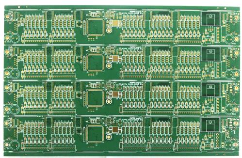
PCB circuit board impedance refers to the parameters of resistance and reactance, which hinder AC power. In the production of PCB circuit boards, impedance processing is essential. The reasons are as follows: 1. PCB circuits (bottom of the board) should consider the installation of electronic components by plugging, and after plugging, issues such as conductivity and signal transmission performance should be considered. Therefore, it is required that the impedance should be as low as possible, and the resistivity should be less than 1&TIMes per square centimeter; Below 10-6. 2. During the production process of PCB circuit boards, they need to go through processes such as copper deposition, electroplating tin (or chemical plating, or thermal spraying tin), and connector soldering. The materials used in these processes must ensure a low resistivity to ensure that the overall impedance of the circuit board meets product quality requirements and can operate normally. 3. The tin plat
Inquiry Now

