 +86 755 2794 4155
  sales@knownpcb.com
-
Shenzhen KNOWNPCB Technology Co., Ltd.
 +86 755 2794 4155
  sales@knownpcb.com
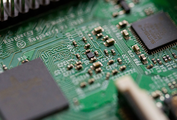
Have you noticed that now more and more of our lighting is using led lighting.What is LED? Compared to the traditional light bulbs, LEDs have lower power consumption, longer lifetime and higher energy efficiency. In the PCB industry,when we say LED PCB, it refers to the pcb used for LED lighting, if you are looking for a suitable LED PCB for your lighting system, this article may bring you something. WHAT ARE LEDS COMPOSED OF?LED is an initial light-emitting diode that produces light when an electric current passes through. LEDs typically have negative and positive electrodes, which generate light in the visible light region.The LEDS are glued to the PCB by soldering process and have electrical connections for lighting.Since light-emitting diodes dissipate a lot of heat when they are in use, when you are designing LED, the metal core is usually the best choice for LED PCB, it is because that it dissipates heat more faster. Among them, the metal material aluminum is the most widely used
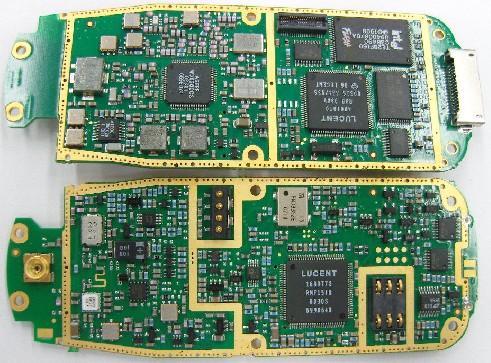
Industrial circuit board damage usually refers to a component being damaged, possibly a chip, a capacitor, or even a small resistor. The repair process involves identifying and replacing the damaged component. 1. Resistors with small resistance values and capacitors with large capacity are prone to damage A resistor with a small resistance value is often used in power supply lines to limit current, which acts as a fuse. If the current is too high, it will first burn out. In addition, many ground capacitors are used in power supply lines for filtering, and their size and capacity are generally large. If the voltage or current is unstable, the capacitors will break down and cause leakage. 2. Fault characteristics and maintenance of capacitor damage The failure caused by capacitor damage is the highest in electronic devices, with electrolytic capacitor damage being the most common. Capacitor damage is manifested as: 1. reduced capacity; 2. Complete loss of capacity; 3. Leakage; 4
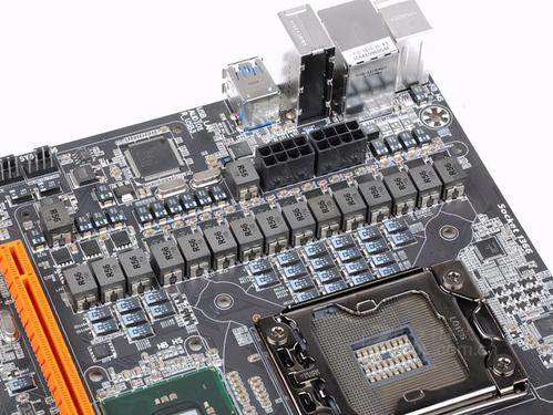
PCB design is an important step before PCB production. If not designed well, it will directly affect the performance and quality of the circuit board, causing the entire circuit board to be scrapped; Layout of components is an important aspect of PCB design. So, what are the requirements for PCB design and layout of components? 1. Aesthetics When designing a PCB, it is not only important to consider the orderly placement of components, but also to consider the graceful and smooth wiring. 2. Force The circuit board should be able to withstand various external forces and vibrations during installation and operation: it should have a reasonable shape, and the positions of various holes on the board should be arranged reasonably; Generally, the distance between the hole and the board edge should be at least greater than the diameter of the hole; It should also be noted that the weakest section of the plate caused by irregular holes should also have sufficient bending strength. 3.
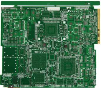
1. Judging the strength level of circuit board manufacturers: Effective PCB sampling before production can also provide a clear understanding of the strength of circuit board manufacturers, especially those who have not cooperated with them before. By sampling, the strength level of circuit board manufacturers in production can be determined. Only circuit board manufacturers with comparable capabilities and the ability to process circuit boards that meet standard technical requirements can be determined, To better meet the requirements of long-term cooperation and high-quality processing and production of PCB boards. 2. Reduce the defect rate in batch production of PCB circuit boards: The processing and production volume of PCB boards are relatively large. In order to ensure smooth mass production without quality problems and reduce defect rates, it is very necessary to conduct circuit board sampling processing before production. The processing of PCB boards requires complex proce
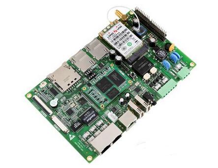
1: When adjusting the mold, please try to use the operation manual instead of relying solely on intuition for operation; 2: Before drilling, check whether the clutch, brake, slider and other parts are normal, whether the operating mechanism is reliable, and confirm all data before performing drilling operations; 3: Several sets of pressure plates and T-head pressure plate screws should be prepared for use corresponding to the mold. The front end of the pressure plate should not contact the straight wall of the lower mold. A piece of sand cloth should be placed between each contact surface, and the screws must be tightened; 4: In order to improve the punching performance of the substrate, the paper substrate should be preheated, with a preferred temperature of 70-90 ℃; 5: Select a punch (including model and tonnage) based on the calculated punching pressure, mold size, and closing height according to the mold design; 6: The gasket under the mold is usually 2 pieces, which must
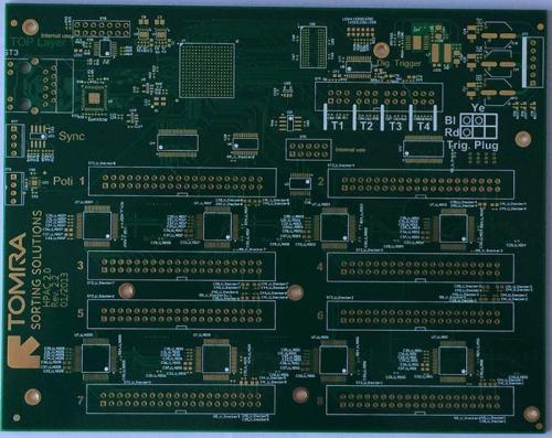
1. Good basic quality/good application effect: The performance of the beloved multi-layer circuit board in terms of basic quality is reassuring, and the direct manifestation is that the electronic products made from it, such as electronic watches, computers, military equipment, etc., are in excellent use. The multi-layer circuit board can excellently complete the interconnection between various electrical components, The quality and texture of high-quality multi-layer boards are evident in various application environments. 2. Outstanding quality/high durability: Users have also found that good multi-layer circuit boards exhibit extremely strong durability, which means they exhibit strong adaptability in various places, including sports facilities. The performance durability and vibration resistance of multi-layer circuit boards are very reassuring. The manufacturing capacity of multi-layer circuit boards is also constantly optimized with the continuous innovation of technology.
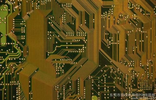
The process of processing PCB multilayer boards is very complex, as it is in the process of laminated boards. The total thickness and number of layers of PCB multilayer boards are limited by the characteristics of the PCB board, and the variety of boards with different thicknesses that special boards can provide is generally limited. Therefore, designers must consider the characteristics of the board and the limitations of the PCB multilayer board processing technology in the PCB multilayer board design process Processing PCB multi-layer board lamination refers to the process of bonding each layer of circuit board into a whole. The process includes: kiss pressing, full pressing, and cold pressing (to quickly cool the circuit board and maintain size stability). During the kiss pressing stage, resin infiltrates the bonding surface and fills the gaps in the circuit, and then enters full pressing to bond all the gaps. The first thing to pay attention to when laminating PCB multilayer b
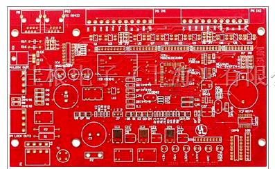
1. Design PCB, create punching files, lay copper plates on both sides of the PCB, then polish the copper plates on both sides for CNC drilling, and inspect for defects after polishing and drying. 2. Main process through hole: To complete the hole, the hole should be sorted and standardized. After confirming that there are no defects in the hole through water washing, drying, and other procedures, black holes should be made to prepare for copper plating through the hole. Next, through holes should be drilled and dried (to ensure sufficient black space, water washing and drying should be performed twice). After completion, copper plating can be carried out. After copper plating, polishing should be carried out, and the hole should be checked again for defects. 3. Production process: apply photosensitive blue oil - dry ink - apply bottom and top line film, and position properly - expose and develop appropriately - wash and dry with water - check for defects in the circuit - tin plat

1. Audio equipment: input and output amplifiers, balanced amplifiers, audio amplifiers, preamplifiers, power amplifiers, etc. 2. Power supply equipment: switch regulators, DC/AC converters, SW regulators, etc. 3. Communication electronic equipment: high-frequency amplifier, filtering device, and transmitting circuit. 4. Office automation equipment: electric motor drivers, etc. 5. Automobile: electronic regulators, igniters, power controllers, etc. 6. Computer: CPU board, floppy disk drive, power supply device, etc. 7. Power module: inverter, solid-state relay, rectifier bridge, etc.
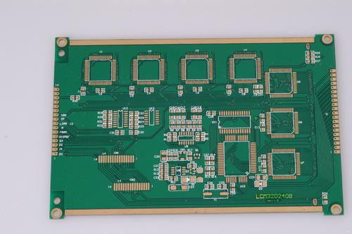
a) Ma Keng: Ma Keng is the result of organic pollution. A large pit usually indicates oil pollution. If the stirring is poor, the bubbles cannot be expelled, which will form pits. Wetting agents can be used to reduce its impact. We usually refer to small pitting as pinholes. Poor pre-treatment, metallic impurities, low boric acid content, and low plating temperature can all cause pinholes. Maintenance and process control of the plating solution are crucial, and anti pinhole agents should be used as process stabilizers to supplement. b) Roughness and burrs: Roughness indicates that the solution is dirty, which can be corrected by sufficient filtration (high pH can easily form hydroxide precipitates and should be controlled). If the current density is too high, impurities are brought in by impure anode mud and added water, and in severe cases, roughness and burrs will be produced. c) Low adhesion: If the copper coating is not fully oxidized, the coating will peel off and the adhesi
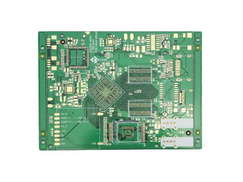
1、 Dry film mask with perforation Many customers believe that after a hole is broken, the film temperature and pressure should be increased to enhance its adhesion. However, this view is not correct because the solvent in the corrosion resistant layer evaporates excessively when the temperature and pressure are too high, making the dry film brittle and thin, making it easy to break through during development. We always need to maintain the toughness of the dry film. Therefore, after a hole is broken, we can improve it from the following points: 1. Reduce film temperature and pressure 2. Improve drilling edge 3. Increase exposure energy 4. Reduce development pressure 5. After applying the film, the parking time should not be too long to avoid causing the semi fluid like drug film at the corner to diffuse and thin under pressure 6. During the film application process, do not tension the dry film too tightly 2、 Penetration occurs during dry film electroplating The reason for
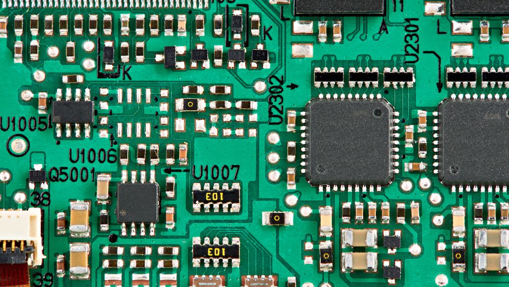
Conducting hole (VIA) is a common type of hole used to conduct or connect copper foil circuits between conductive patterns in different layers of a circuit board. For example, blind holes or buried holes, but cannot be inserted into copper plated holes of component leads or other reinforcement materials. Because PCBs are formed by stacking and accumulating many layers of copper foil, an insulation layer is laid between each layer of copper foil, so the copper foil layers cannot communicate with each other, and their signal connections rely on through holes (via), hence the Chinese name for through holes. The characteristic is that in order to meet the needs of customers, the conductive holes on the circuit board need to be plugged. This changes the traditional aluminum sheet plugging process by using white mesh to complete the circuit board surface solder mask and plug holes, making it stable in production, reliable in quality, and more perfect in use. Conducting holes mainly serv

1. Report the results of the work The leader who lifts the heavy weight is the favorite. When reporting work, please remember to report the result to the leader first, and the result thinking is the first thinking. 2. Ask for work plan Please ensure that at least two programs are given to leaders, and express their views and effective suggestions. Don't let the leader do the quiz questions, but let the leader do the multiple-choice questions. Don't ask the leader how to do this thing, what to do, but ask, I have a plan, you can listen to it and see how it goes! 3. Summarize the work process and find three points To do a work summary, it is necessary to describe the process, not only to have a clear sequence and logic, but also to find out the key points, mistakes, and reflection points in the process. 4. Arrange work standards and clarify customer requirements Layout work must be clear about customer requirements and quality standards, otherwise subordinates will not know how
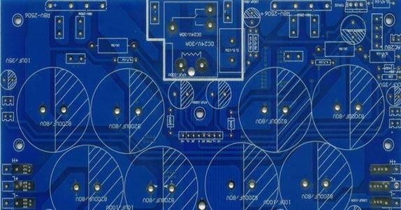
After the customer's plug-in test, it is found that the via hole (via hole) is not connected. The test can be carried out normally before the plug-in, and the appearance has no drilling deviation phenomenon, which is mainly caused by the following five reasons: First: the hole copper is not enough; Second: the roughness of the hole wall is too large Third: Drilling dust plug holes Fourth: drilling broken knife to make up holes Fifth: poor solder mask plug hole In terms of controlling the problem of through-hole failure, the hole copper is the most important link. The automatic sinking copper line of our Honglian circuit is not small: Detection: The detection method of immersion copper wire is mainly backlight series detection. The number of series is more than 9 to be qualified to ensure the quality of copper immersion and hole formation. The detection methods include deposition speed force detection (copper layer thickness in standard time); glue removal speed force (this

One, circuit board factory tin surface quality defects So what are the factors that cause the bad tin surface of the tin surface? According to the analysis of the editor, there are the following points 1. The operation is not in accordance with the operating specifications when shipping The circuit industry has extremely strict requirements on the workshop environment and the standard operation of employees, especially the chemical reaction environment is required in the circuit board production process, so the infiltration of impurities is not allowed. After the board spraying process is completed, the subsequent one All series require employees to wear anti-static gloves to operate, because finger sweat or stains directly contact the surface, which will cause surface oxidation. If it causes defects, it is extremely difficult to find, and it is irregular, and it is difficult to be exposed in testing and tinning experiments. 2. The tin furnace for spraying tin is not cleaned on

The transmission rate of high-speed PCB design wiring systems is constantly accelerating with the passage of time, but this also brings a new challenge - the anti-interference ability is becoming weaker and weaker. All of this stems from the fact that the higher the frequency of information transmission, the more sensitive the signal, and the weaker the energy, making the wiring system increasingly susceptible to interference. In some common electronic devices, such as computer screens, mobile phones, motors, radio broadcasting equipment, etc., cables and devices can interfere with other components or be severely interfered by other interference sources. Today, let me introduce a shielding method in high-frequency PCB design to you, let's take a look together! Especially when using high-speed data networks, the time required to intercept a large amount of information is significantly lower than the time required to intercept low-speed data transmission. The twisted pair in data twis
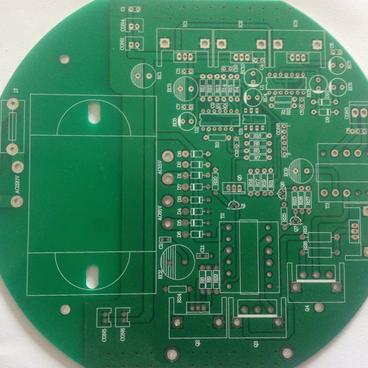
High frequency PCB circuit board is a special type of circuit board with high electromagnetic frequency. Generally speaking, high frequency can be defined as a frequency above 1GHz. Its various physical properties, accuracy, and technical parameters require very high requirements, and are commonly used in fields such as automotive collision prevention systems, satellite systems, and radio systems. Wireless infrastructure needs to provide sufficiently low insertion loss in order to effectively improve energy utilization efficiency. With the arrival of 4G services, RF products need to provide wider bandwidth and be compatible with 3G and 2G services. PCB sample manufacturers believe that at the same time, base stations are becoming smaller and lighter, and are installed on top of towers, which is also promoting the development of miniaturization of circuit boards. Many manufacturers are seeking materials that can miniaturize antennas in handheld devices such as tablets. Optimistic

Q: How to conduct pilot testing on PCB circuit boards? Answer: Today, electronic products are becoming thinner and shorter, and the preset wiring of PCBs is becoming more complex and difficult. In addition to balancing functionality and safety, it is also necessary to be producible and testable. We hereby provide a rule for the reference of the preset wiring engineer regarding the need for measurability. Kunshan circuit board sampling manufacturers believe that if they pay attention to it, it will save your company considerable tooling production costs and promote the reliability of testing and the service life of fixtures. Although there is a double-sided fixture, it is preferable to place the measured point on a unified surface. The important consideration is to be able to perform single-sided testing. If there is difficulty, the TOP SIZE needle points should be less than the BOTTON SIZE. 2. Priority of measurement points: I Test pad II Component lead III Via hole -->but not
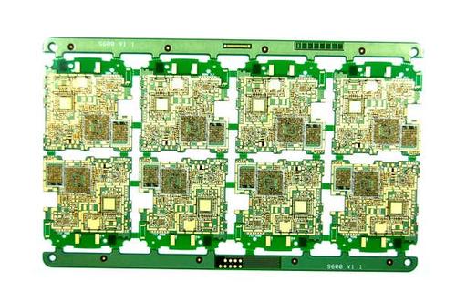
Key components require preset test points on the PCB circuit board. The solder pads used for welding appearance assembly components are not allowed to be used as inspection points. A dedicated test solder pad must be pre-set to ensure smooth solder joint inspection and production debugging. The solder pads used for testing should be arranged on the unified side of the PCB circuit board as much as possible, which is beneficial for testing and reduces the cost of testing. The following circuit board sample manufacturer will tell you its process preset requirements: (1) The distance between test points and the edge of the PCB circuit board should be greater than 5mm; (2) The test point should not be covered by solder mask or text ink; (3) The testing point should be preferably coated with solder or selected with a soft, easy to penetrate, and non oxidizing metal to ensure reliable grounding and extend the service life of the probe (4) The testing point should be placed 1mm away fr
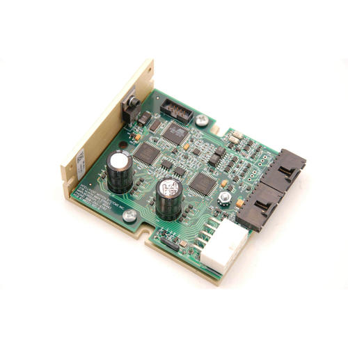
PCBA test stand is a device used to test PCBA finished products. When making PCBA test racks, PCBA processing plants usually need to provide Gerber files and PCBA samples to facilitate the production of test racks. For the current PCBA test bench, only a few pressure plate buckles are installed on the test bench, and the PCBA is fixed by a thimble and pressure plate buckle. During the PCBA function test, press the PCBA into the pressure plate buckle with both hands. Due to uneven force or insufficient compression, PCBA can easily cause poor contact between the testing needle and PCBA, seriously affecting testing efficiency and accuracy; If too much force is applied, it is easy to deform or damage the PCBA when pressing down, and it is also easy to damage the test needle of the testing frame, causing significant losses. 1、 Material preparation After determining the plan based on the information, it is necessary to prepare hardware materials (electronic components), relevant additi
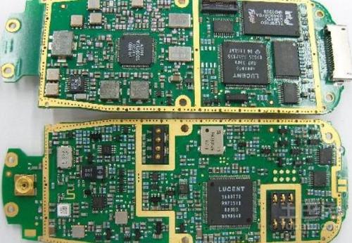
Aluminum substrate is a unique metal based copper clad plate with good thermal conductivity, electrical insulation performance, and mechanical processing performance. Let the aluminum substrate manufacturer provide you with a detailed explanation of the aluminum substrate. 1、 Characteristics of aluminum substrate 1. Adopting Surface Mount Technology (SMT); 2. Effectively handle thermal diffusion in circuit design schemes; 3. Reduce product operating temperature, improve product power density and reliability, and extend product service life; 4. Reduce product volume, reduce hardware and assembly costs; 5. Replace fragile ceramic substrates for better mechanical durability. 2、 Structure of aluminum substrate Aluminum based copper clad plate is a metal circuit board material composed of copper foil, thermal insulation layer, and metal substrate: Copper foil: equivalent to a copper clad board of a regular PCB, with a copper foil thickness of loz to 10oz for the circuit. Therm
Inquiry Now

