 +86 755 2794 4155
  sales@knownpcb.com
-
Shenzhen KNOWNPCB Technology Co., Ltd.
 +86 755 2794 4155
  sales@knownpcb.com
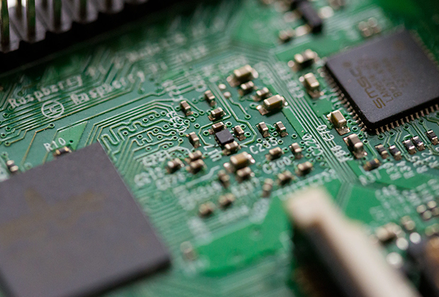
Have you noticed that now more and more of our lighting is using led lighting.What is LED? Compared to the traditional light bulbs, LEDs have lower power consumption, longer lifetime and higher energy efficiency. In the PCB industry,when we say LED PCB, it refers to the pcb used for LED lighting, if you are looking for a suitable LED PCB for your lighting system, this article may bring you something. WHAT ARE LEDS COMPOSED OF?LED is an initial light-emitting diode that produces light when an electric current passes through. LEDs typically have negative and positive electrodes, which generate light in the visible light region.The LEDS are glued to the PCB by soldering process and have electrical connections for lighting.Since light-emitting diodes dissipate a lot of heat when they are in use, when you are designing LED, the metal core is usually the best choice for LED PCB, it is because that it dissipates heat more faster. Among them, the metal material aluminum is the most widely used
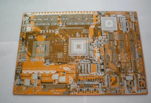
The main purpose of vacuum aluminum coating film is to replace pure aluminum foil composite, giving soft packaging printed materials an elegant silver white luster, and reducing packaging printing costs while improving the barrier and shading properties of soft packaging film bags (aluminum coating film instrument is 0.4~0.6) μ m. Only about 1/150) 25% of the amount of pure aluminum foil used. The PCB sampling manufacturer tells you that there are two common vacuum aluminum plating methods: One is vacuum aluminum plating after printing, which involves reverse inner printing on the surface of the thin film, followed by aluminum plating, and then composite with the bottom film; The second is to directly imprint on the surface of the thin film, and then dry composite it with the vacuum aluminum plated bottom film. But this method requires the use of materials such as CPP and PE with good heat resistance and heat sealing for the bottom film. No matter what method is used, the compo
1. Industry regulatory authorities and regulatory system The Ministry of Industry and Information Technology of China is the competent department in charge of the printed circuit board industry. Its main responsibilities include formulating and organizing the implementation of industry plans, plans, and policies for the industrial and communication industries, proposing policy recommendations for optimizing industrial layout and structure, drafting relevant laws and regulations, formulating regulations, drafting industry technical specifications and standards, and organizing their implementation, guiding industry quality management work. The Electronic Information Department under the Ministry of Industry and Information Technology of China is responsible for industry management of electronic information product manufacturing; Organize and coordinate the development and production of major system equipment, microelectronics and other basic products, and organize and coordinate the
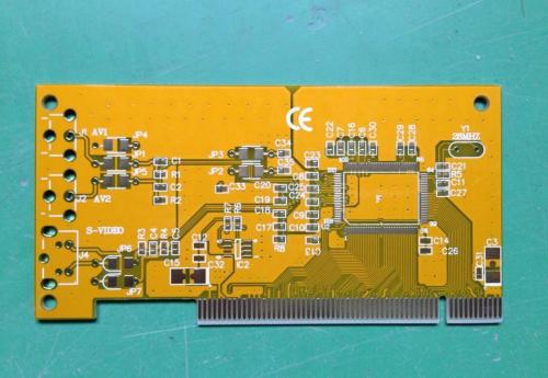
Negative film of circuit board: Generally speaking, it is the tenting process that uses acidic etching negative film because after the film is made, the desired circuit or copper surface is transparent, while the unwanted parts are black. After exposure by the circuit process, the transparent part hardens chemically due to the exposure of the dry film inhibitor to light. The subsequent development process will wash away the dry film that has not hardened, So in the etching process, only a portion of the copper foil (the black part of the film) that has been washed off by biting off the dry film is retained, while the circuit (the transparent part of the film) that belongs to our desired circuit (PCB sample) is retained. We will tell you about the positive of the circuit board. Generally, this is the pattern process we are talking about, and the solution used is alkaline etching positive. If viewed from the negative, the desired circuit or copper surface is black, while the other pa
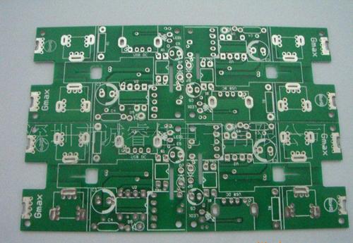
The earlier the signal integrity (SI) problem is solved, the higher the efficiency of the design, which can avoid adding termination devices only after the circuit board design is completed. There are many tools and resources available for SI design planning. This article explores the core issues of signal integrity and several methods to solve SI problems, ignoring the technical details of the design process. With the increase of IC output switching speed, almost all designs have encountered signal integrity issues regardless of the signal cycle. Even if you haven't encountered SI issues in the past, as the working frequency of the circuit increases, you will definitely encounter signal integrity issues in the future. The signal integrity problem mainly refers to the phenomenon of signal overshoot and damping oscillation, which are mainly functions of IC driving amplitude and jump time. That is to say, even if the wiring topology remains unchanged, as long as the chip speed beco
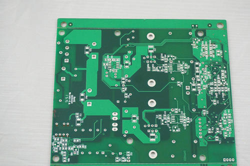
1. Engineering design: Precautions for printed circuit board design: A. The arrangement of interlayer semi cured sheets should be symmetrical, for example, for a six layer board, the thickness and number of semi cured sheets between layers 1-2 and 5-6 should be consistent, otherwise it is easy to warp after lamination. B. Multi layer core boards and semi cured sheets should use products from the same supplier. C. The area of the circuit diagram on the outer A and B sides should be as close as possible. If side A is a large copper surface and side B only runs a few wires, this type of printed circuit board is prone to warping after etching. If the area difference between the two sides of the circuit is too large, independent grids can be added to the sparse side for balance. 2. Drying board before cutting: The purpose of drying the copper-clad board before cutting (150 degrees Celsius, time 8 ± 2 hours) is to remove moisture from the board and completely cure the resin inside t
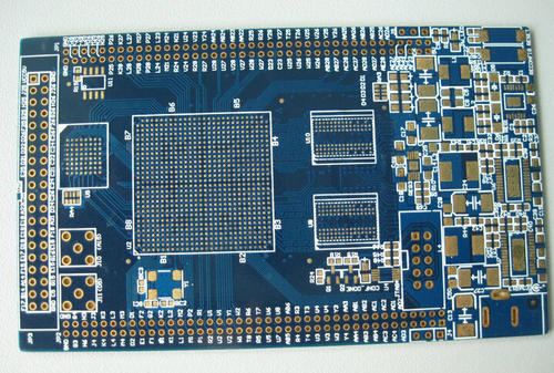
1、 Why do circuit boards require a very flat surface The circuit board prototype manufacturer tells you that if the printed circuit board is not flat on the automated insertion line, it will cause inaccurate positioning, prevent components from being inserted into the holes and surface mounting pads of the board, and even damage the automatic insertion machine. The board where the components are installed is bent after welding, making it difficult to cut the component legs flat and neat. The board cannot be installed on the chassis or socket inside the machine, so it is also very troublesome for the assembly plant to encounter board warping. At present, printed boards have entered the era of surface installation and chip installation, and assembly plants are bound to have increasingly strict requirements for board warping. 2、 Standards and testing methods for warpage According to the American IPC-6012 (1996 edition), the allowable large warpage and distortion for surface mount
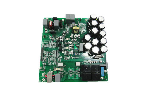
The positioning of CNC milling is to use positioning pins to position the printed circuit board to be processed on the workbench of the milling machine, so as to conveniently and accurately process the shape of the printed circuit board. Require simple and reliable positioning, capable of quickly loading and unloading boards while eliminating chips. The manufacturer of circuit board samples tells you that there are various positioning methods, such as the design of reciprocating workbenches for some milling machines. When one worktable is being processed, the other worktable loads and unloads the board. There is also a method of using two sets of milling positioning pads. When one milling positioning pad is processed on the CNC milling workbench, the other milling positioning pad is loaded and unloaded on the platform. The exchange between the two only takes a few seconds. The CNC milling worktable itself is a positioning plate, which is an aluminum alloy plate fixed with pins and
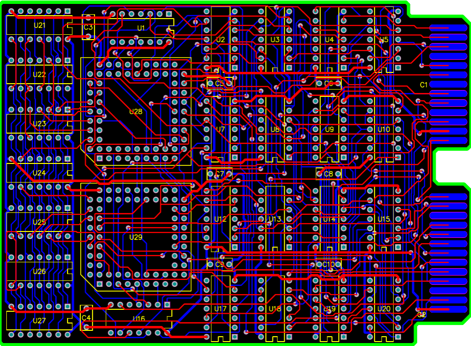
In circuit design, we are generally concerned about signal quality issues, but sometimes we limit our research to signal lines and treat power and ground as ideal situations. Although this approach can simplify the problem, it is no longer feasible in high-speed design. Although the direct result of circuit design is reflected in signal integrity, we cannot ignore power integrity design as a result. Because the integrity of the power supply directly affects the signal integrity of the subsequent PCB board. Power integrity and signal integrity are closely related, and in many cases, PCB sample manufacturers believe that the main cause of signal distortion is the power system. For example, excessive ground rebound noise, inappropriate design of decoupling capacitors, severe circuit impact, poor separation of multiple power sources/ground planes, unreasonable geological design, uneven current, and so on. 1) Power distribution system Power integrity design is a very complex task, but i
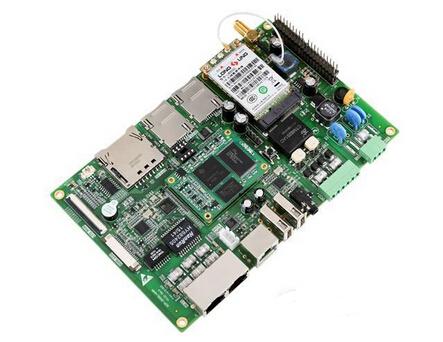
In commercial production, there are two laser technologies available for laser drilling. The wavelength of CO2 laser is in the far-infrared band, and the wavelength of ultraviolet laser is in the ultraviolet band. CO2 laser is widely used in the production of industrial micro through-holes on printed circuit boards, with a requirement that the diameter of the micro through-hole be greater than 100 μ (Raman, 2001). For the production of these large aperture holes, CO2 laser has high productivity because the punching time required for CO2 laser to produce large holes is very short. UV laser technology is widely used in diameters less than 100 μ In the production of micro pores in m, with the use of miniaturized circuit diagrams, the pore size can even be less than 50 μ M. Ultraviolet laser technology in the production of diameters less than 80 μ The yield of m holes is very high. Therefore, in order to meet the increasing demand for microporous productivity, many manufacturers have b
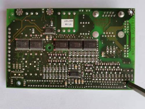
CO2 laser effectively removes dielectrics, even non-uniform glass reinforced dielectrics. However, a single CO2 laser cannot create small holes (less than 75 μ m) In addition to removing copper, Suzhou circuit board sample manufacturers believe that there are also a few exceptions, which are that it can remove pre processed 5 μ Thin copper foil below m (Lustino, 2002). UV laser can create very small holes and remove all ordinary copper streets (3-36 μ m. 1oz, even electroplated copper foil. UV laser can also remove dielectric materials separately, but at a slower speed. Moreover, for non-uniform materials, such as reinforced glass FR-4, the effect is usually not good. This is because only when the energy density is increased to a certain extent can the glass be removed, which will also damage the inner solder pads. Due to the fact that the stick laser system includes ultraviolet laser and CO2 laser, it can achieve better results in both fields. UV laser can complete all copper foil
1. Report the results of the work The leader who lifts the heavy weight is the favorite. When reporting work, please remember to report the result to the leader first, and the result thinking is the first thinking. 2. Ask for work plan Please ensure that at least two programs are given to leaders, and express their views and effective suggestions. Don't let the leader do the quiz questions, but let the leader do the multiple-choice questions. Don't ask the leader how to do this thing, what to do, but ask, I have a plan, you can listen to it and see how it goes! 3. Summarize the work process and find three points To do a work summary, it is necessary to describe the process, not only to have a clear sequence and logic, but also to find out the key points, mistakes, and reflection points in the process. 4. Arrange work standards and clarify customer requirements Layout work must be clear about customer requirements and quality standards, otherwise subordinates will not know ho
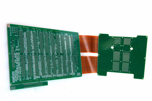
After the customer's plug-in test, it is found that the via hole (via hole) is not connected. The test can be carried out normally before the plug-in, and the appearance has no drilling deviation phenomenon, which is mainly caused by the following five reasons: First: the hole copper is not enough; Second: the roughness of the hole wall is too large Third: Drilling dust plug holes Fourth: drilling broken knife to make up holes Fifth: poor solder mask plug hole In terms of controlling the problem of through-hole failure, the hole copper is the most important link. The automatic sinking copper line of our Honglian circuit is not small: Detection: The detection method of immersion copper wire is mainly backlight series detection. The number of series is more than 9 to be qualified to ensure the quality of copper immersion and hole formation. The detection methods include deposition speed force detection (copper layer thickness in standard time); glue removal speed force (this
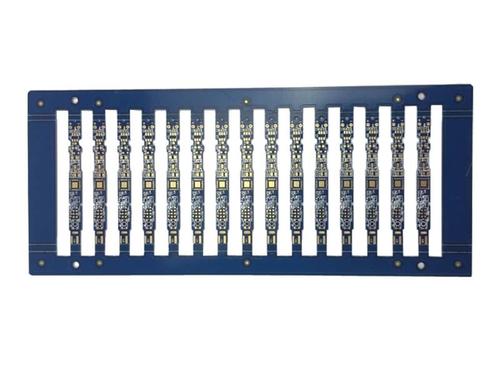
One, circuit board factory tin surface quality defects So what are the factors that cause the bad tin surface of the tin surface? According to the analysis of the editor, there are the following points 1. The operation is not in accordance with the operating specifications when shipping The circuit industry has extremely strict requirements on the workshop environment and the standard operation of employees, especially the chemical reaction environment is required in the circuit board production process, so the infiltration of impurities is not allowed. After the board spraying process is completed, the subsequent one All series require employees to wear anti-static gloves to operate, because finger sweat or stains directly contact the surface, which will cause surface oxidation. If it causes defects, it is extremely difficult to find, and it is irregular, and it is difficult to be exposed in testing and tinning experiments. 2. The tin furnace for spraying tin is not cleaned on
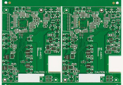
However, due to fierce market price competition, the cost of circuit board prototype materials is also on the rise. More and more manufacturers are monopolizing the market with low prices in order to enhance their core competitiveness. However, behind these ultra-low prices, they are obtained by reducing material and process manufacturing costs. However, devices are often prone to cracks (cracks), scratches, (or abrasions), and their precision, performance, and other comprehensive factors are not up to standard, seriously affecting the solderability and reliability of products used. Facing the diverse types of circuit board samples on the market, identifying the quality of circuit board samples can be approached from two aspects; One method is to judge based on appearance, and the other is to judge based on the quality specifications of the PCB board itself. 1. Standard rules for size and thickness. The thickness of a circuit board is different from that of a standard circuit boar

The price of PCB has always been a confusing issue for many buyers, and many people may wonder how these prices are calculated when placing orders online. Below, PCB sample manufacturers will discuss the composition factors of PCB prices together. 1. The diversity of prices caused by different materials used in PCBs. For example, ordinary double-sided boards generally have FR4 (Shengyi, Jiantao, Guoji, three prices from top to bottom), with board thicknesses ranging from 0.2mm to 3.0mm and copper thicknesses ranging from 0.5oz to 3oz, all of which cause significant price differences in board materials; In terms of solder mask ink, there is also a certain price difference between ordinary thermosetting oil and photosensitive green oil. 2. Common causes of price diversity due to different surface treatment processes include OSP (oxidation resistance), lead spray tin, lead-free spray tin (environmental protection), gold plating, gold deposition, and some combination processes, among
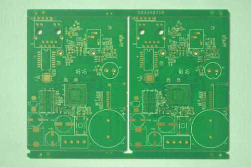
1. The issue of cleanliness of the board surface; 2. The issue of surface micro roughness (or surface energy). The blistering problem on all circuit boards can be summarized as the above reasons. Poor or too low adhesion between coatings makes it difficult to resist the coating stress, mechanical stress, and thermal stress generated during subsequent production and assembly processes, resulting in varying degrees of separation between coatings. The factors that may cause poor surface quality during the production and processing process are summarized as follows: 1. Issues with substrate processing: Especially for some thinner substrates (generally below 0.8mm), due to poor substrate rigidity, it is not suitable to use a brush machine to brush the substrate. This may not effectively remove the protective layer specially treated to prevent oxidation of the copper foil on the surface of the substrate during production and processing. Although this layer is thin and easy to remove b
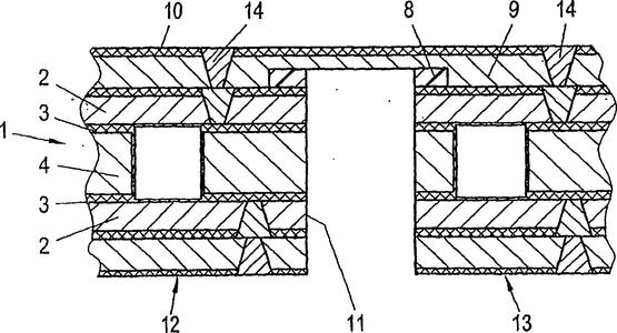
1、 Dry film mask with perforation Many customers believe that after a hole is broken, the film temperature and pressure should be increased to enhance its adhesion. However, this view is not correct because the solvent in the corrosion resistant layer evaporates excessively when the temperature and pressure are too high, making the dry film brittle and thin, making it easy to break through during development. We always need to maintain the toughness of the dry film. Therefore, after a hole is broken, we can improve it from the following points: 1. Reduce film temperature and pressure 2. Improve drilling edge 3. Increase exposure energy 4. Reduce development pressure 5. After applying the film, the parking time should not be too long to avoid causing the semi fluid like drug film at the corner to diffuse and thin under pressure 6. During the film application process, do not tension the dry film too tightly 2、 Penetration occurs during dry film electroplating The reason for
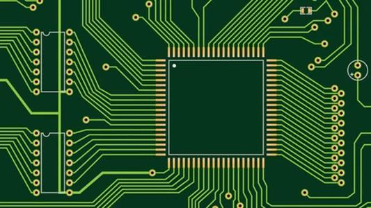
a) Ma Keng: Ma Keng is the result of organic pollution. A large pit usually indicates oil pollution. If the stirring is poor, the bubbles cannot be expelled, which will form pits. Wetting agents can be used to reduce its impact. We usually refer to small pitting as pinholes. Poor pre-treatment, metallic impurities, low boric acid content, and low plating temperature can all cause pinholes. Maintenance and process control of the plating solution are crucial, and anti pinhole agents should be used as process stabilizers to supplement. b) Roughness and burrs: Roughness indicates that the solution is dirty, which can be corrected by sufficient filtration (high pH can easily form hydroxide precipitates and should be controlled). If the current density is too high, impurities are brought in by impure anode mud and added water, and in severe cases, roughness and burrs will be produced. c) Low adhesion: If the copper coating is not fully oxidized, the coating will peel off and the adhesi
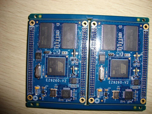
Conducting hole (VIA) is a common type of hole used to conduct or connect copper foil circuits between conductive patterns in different layers of a circuit board. For example, blind holes or buried holes, but cannot be inserted into copper plated holes of component leads or other reinforcement materials. Because PCBs are formed by stacking and accumulating many layers of copper foil, an insulation layer is laid between each layer of copper foil, so the copper foil layers cannot communicate with each other, and their signal connections rely on through holes (via), hence the Chinese name for through holes. The characteristic is that in order to meet the needs of customers, the conductive holes on the circuit board need to be plugged. This changes the traditional aluminum sheet plugging process by using white mesh to complete the circuit board surface solder mask and plug holes, making it stable in production, reliable in quality, and more perfect in use. Conducting holes mainly serv
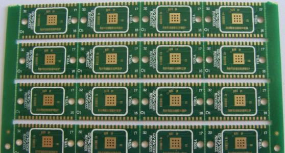
First, it is equal length. When designing a differential line, pay attention to making the lengths of the two signal lines the same. Because the length of the signal lines is the same, the transmission time of the signals is also the same, so the polarities of the differential signals will be different, resulting in the opposite situation. If the differential signal is the same, the signal quality will be poor.Next, is the isometric. That is to say, the distance between pairs of differential lines should be consistent. By adjusting the distance of the differential line, we can adjust a differential impedance in the whole process. What is the benefit of doing this? If our differential impedance can maintain a certain continuity, then there will be very few reflections and the transmitted signal will be very complete.Finally, it is the stacking of differential lines and printed boards. It is generally believed that the differential line will provide a reflow path for the printed board, a
Inquiry Now

