 +86 755 2794 4155
  sales@knownpcb.com
-
Shenzhen KNOWNPCB Technology Co., Ltd.
 +86 755 2794 4155
  sales@knownpcb.com
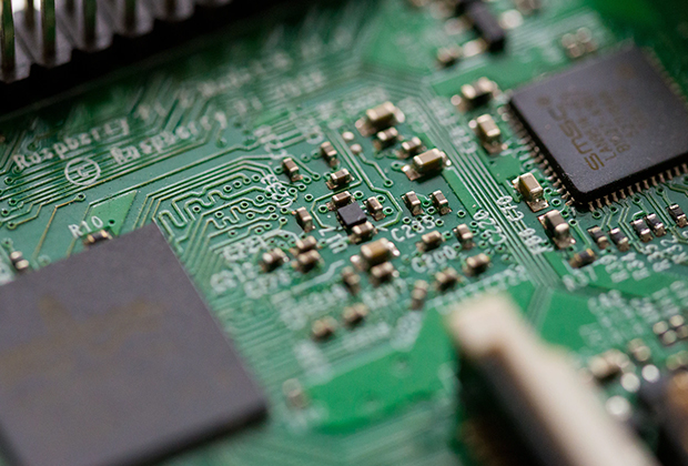
Have you noticed that now more and more of our lighting is using led lighting.What is LED? Compared to the traditional light bulbs, LEDs have lower power consumption, longer lifetime and higher energy efficiency. In the PCB industry,when we say LED PCB, it refers to the pcb used for LED lighting, if you are looking for a suitable LED PCB for your lighting system, this article may bring you something. WHAT ARE LEDS COMPOSED OF?LED is an initial light-emitting diode that produces light when an electric current passes through. LEDs typically have negative and positive electrodes, which generate light in the visible light region.The LEDS are glued to the PCB by soldering process and have electrical connections for lighting.Since light-emitting diodes dissipate a lot of heat when they are in use, when you are designing LED, the metal core is usually the best choice for LED PCB, it is because that it dissipates heat more faster. Among them, the metal material aluminum is the most widely used
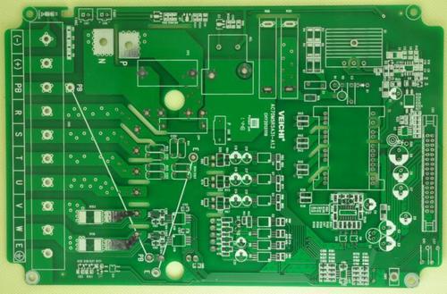
1. If the PCB has a large amount of ground, such as SGND, AGND, GND, etc., it is necessary to use the most important "ground" as the reference for independent copper coating based on the different positions of the PCB surface. Separate the digital and analog power lines for copper coating, and before copper coating, thicken the corresponding power lines: 5.0V, 3.3V, etc. 2. For single point connections to different locations, the method is to connect through a 0 ohm resistor, magnetic bead, or inductor. 3. The crystal oscillator in the circuit is a high-frequency emission source. For the copper coating near the crystal oscillator, the method is to surround the crystal oscillator with copper coating, and then ground the outer shell of the crystal oscillator separately. 4. If the problem of islands (dead zones) is significant, then define a place and add it through a hole. 5. When starting wiring, the ground wire should be treated equally. When wiring, the ground wire should be pro
During the production process of PCB circuit boards, it is common to encounter poor copper wire detachment, also known as copper throwing, which affects product quality. So, what are the common reasons for PCB circuit board copper throwing? 1、 PCB process factors: 1. Copper foil is excessively etched, and the electrolytic copper foil used in the market is generally single-sided galvanized (commonly known as ashed foil) and single-sided copper plating (commonly known as reddened foil). The common copper throwing is generally ashed foil above 70um, while reddened foil and ashed foil below 18um have not undergone bulk copper throwing. 2. Local collisions occurred during the PCB process, causing the copper wire to detach from the substrate due to external mechanical forces. This defect manifests as poor positioning or directionality, where the detached copper wire will have obvious twisting or scratches/impact marks in the same direction. 3. Unreasonable PCB circuit design, using t

The so-called copper coating of PCB circuit boards refers to using the idle space on the PCB as a reference plane, and then filling it with solid copper. These copper areas are also known as copper filling. The significance of copper coating is to reduce the impedance of the ground wire and improve its anti-interference ability; Reduce voltage drop and improve power efficiency; Connecting to the ground wire can also reduce the loop area. There are generally two methods of copper coating, namely large-scale copper coating and grid copper coating. Large area copper coating has the dual functions of increasing current and shielding, but if the copper coating is applied on a large area, the board may curl up and even bubble during wave soldering. Therefore, when covering a large area with copper, several grooves are usually opened to alleviate blistering on the copper foil. Grid copper coating, from the perspective of heat dissipation, reduces the heating surface of copper and plays a
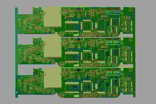
Electrical principles and mechanical structure design, determining the size and structural shape of the PCB based on the overall structure of the machine. Draw a process diagram of the SMT printed circuit board, indicating the length, width, and thickness of the PCB, the position and size of structural components and assembly holes, and leaving edge dimensions, so that circuit designers can carry out wiring design within an effective range. The choice of assembly form depends on the type of components in the circuit, the size of the circuit board, and the equipment conditions of the production line. PCB board sampling shares with you the principles for selecting the assembly form of printed boards: following the principles of optimizing processes, reducing costs, and improving product quality, first determine the overall goals of electronic product functions, performance indicators, costs, and overall dimensions of the entire machine. When developing and designing new products, th
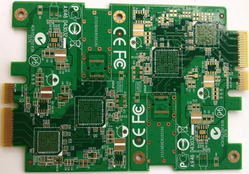
Pre impregnated material is a sheet-like material composed of resin and carrier. Among them, the resin is in the B-stage, under the action of temperature and pressure, it has fluidity and can quickly cure and complete the bonding process, and together with the carrier, forms an insulation layer. Commonly known as semi cured sheet or adhesive sheet. To ensure the high reliability and quality stability of multi-layer printed circuit boards, it is necessary to conduct quality testing on the characteristics of semi-solid chips (test layer pressing method). The characteristics of electroplating semi cured chips on circuit boards include two parts: pre lamination characteristics and post lamination characteristics. The characteristics before lamination mainly refer to: resin content%, fluidity%, volatile content% and gel time (S). The circuit board prototype manufacturer will share with you the characteristics after lamination, including electrical performance, thermal shock performance,
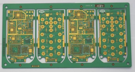
1. Process half of the hole with a double V-shaped cutting tool. 2. Second drill adds support holes at the edge of the hole, removes copper skin in advance, reduces burrs, and uses slot cutters to produce the drill, optimizing the speed and falling speed. 3. Copper plating is applied to the substrate by depositing a layer of copper on the hole wall of the circular holes on the edge of the board. 4. After laminating, exposing, and developing the outer circuit, the substrate is subjected to secondary copper plating and tin plating to thicken the copper layer on the hole wall of the circular hole at the edge of the board and cover it with a tin layer with anti-corrosion properties; 5. Half hole forming involves cutting the circular holes on the edge of the board in half to form a half hole; 6. Remove the anti electroplating film pressed during the process of film removal and pressing; 7. Etching is performed on the substrate to remove the exposed copper on the outer layer of the
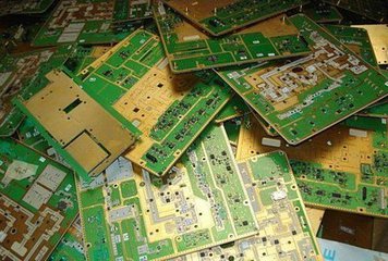
a) Ma Keng: Ma Keng is the result of organic pollution. A large pit usually indicates oil pollution. If the stirring is poor, the bubbles cannot be expelled, which will form pits. Wetting agents can be used to reduce its impact. We usually refer to small pitting as pinholes. Poor pre-treatment, metallic impurities, low boric acid content, and low plating temperature can all cause pinholes. Maintenance and process control of the plating solution are crucial, and anti pinhole agents should be used as process stabilizers to supplement. b) Roughness and burrs: Roughness indicates that the solution is dirty, which can be corrected by sufficient filtration (high pH can easily form hydroxide precipitates and should be controlled). If the current density is too high, impurities are brought in by impure anode mud and added water, and in severe cases, roughness and burrs will be produced. c) Low adhesion: If the copper coating is not fully oxidized, the coating will peel off and the adhesi
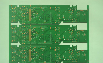
1、 Dry film mask with perforation Many customers believe that after a hole is broken, the film temperature and pressure should be increased to enhance its adhesion. However, this view is not correct because the solvent in the corrosion resistant layer evaporates excessively when the temperature and pressure are too high, making the dry film brittle and thin, making it easy to break through during development. We always need to maintain the toughness of the dry film. Therefore, after a hole is broken, we can improve it from the following points: 1. Reduce film temperature and pressure 2. Improve drilling edge 3. Increase exposure energy 4. Reduce development pressure 5. After applying the film, the parking time should not be too long to avoid causing the semi fluid like drug film at the corner to diffuse and thin under pressure 6. During the film application process, do not tension the dry film too tightly 2、 Penetration occurs during dry film electroplating The reason for
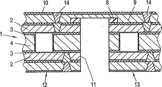
In terms of electrical performance, it includes dielectric constant and loss angle, ① dielectric constant or dielectric coefficient, and the surface is a coefficient of insulation capacity characteristics, measured in units of ε In actual production, the dielectric constant is not an absolute value, but expressed in the form of relative dielectric constant The loss angle, also known as the "loss factor" or "damping factor", is the tangent of the phase difference angle between the strain and stress cycles of a material in the residual alternating field, which is also equal to the ratio of the loss film amount of the material to the stored energy modulus. Thermal performance method: It is necessary to have a certain understanding of the relevant characteristic parameters. Below, we will introduce the definition manual of thermal performance parameters for two different sheet materials: ① From the perspective of board types alone, it can be mainly divided into Tg value, Td value, CT
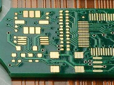
① Inner layer production: Multilayer circuit boards are made by pressing two or more double-sided boards. For some high-frequency multi-layer boards, the inner layer holes may be blind holes, and the inner layer boards need to be drilled and then pressed together. ② Drilling: Based on the production capacity of the factory, verify the data. If the line width moment or aperture is less than the manufacturing capacity, the engineering department should improve communication with the customer and reach a consensus to compensate for a certain stroke of the line width moment or aperture. Generally, the drilling roughness is controlled at ≤ 25.4um. ③ Copper plating: Usually, during transportation or production, there may be scratches on the substrate copper foil, causing it to be exposed to the surface. It is necessary to go through processes such as copper plating to ensure that the thickness of the PCB board copper foil meets the customer's order requirements. Secondly, according to

1. IPC/EIA/JEDECJ-STD-003A: Solderability testing for customized circuit boards. 2. IPC-6018A: Manufacturing inspection and testing of microwave finished circuit boards, including manufacturing performance and qualification requirements for high-frequency circuit boards. 3. IPC-M-103: Surface Mount Assembly Manual Standard, which includes all 21 IPC documents related to PCB surface mount. 4. IPC-M-I04: PCB Manufacturing and Assembly Manual Standard, which includes the 10 most widely used documents related to circuit board manufacturing and assembly. 5. IPC-DRM-53: Introduction to Electronic PCB Assembly Desktop Reference Manual, with illustrations and photos describing through-hole installation and surface mount assembly techniques. 6. IPC-Ca-821: General requirements for thermal conductive adhesives, including requirements and testing methods for thermal conductive dielectrics that bond components to appropriate positions. 7. IPC-3406: Guidelines for Conductive Surface Coati
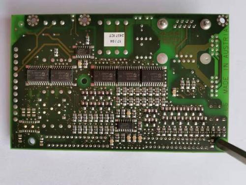
During the production process of PCB circuit boards, it is common to encounter poor copper wire detachment, also known as copper throwing, which affects product quality. So, what are the common reasons for PCB circuit board copper throwing? 1、 PCB process factors: 1. Copper foil is excessively etched, and the electrolytic copper foil used in the market is generally single-sided galvanized (commonly known as ashed foil) and single-sided copper plating (commonly known as reddened foil). The common copper throwing is generally ashed foil above 70um, while reddened foil and ashed foil below 18um have not undergone bulk copper throwing. 2. Local collisions occurred during the PCB process, causing the copper wire to detach from the substrate due to external mechanical forces. This defect manifests as poor positioning or directionality, where the detached copper wire will have obvious twisting or scratches/impact marks in the same direction. 3. Unreasonable PCB circuit design, using t
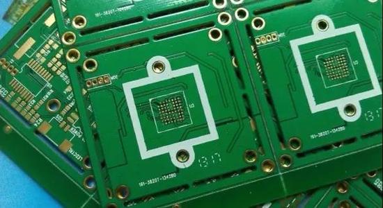
Aluminum substrate is a unique metal based copper clad plate with good thermal conductivity, electrical insulation performance, and mechanical processing performance. Let the aluminum substrate manufacturer provide you with a detailed explanation of the aluminum substrate. 1、 Characteristics of aluminum substrate 1. Adopting Surface Mount Technology (SMT); 2. Effectively handle thermal diffusion in circuit design schemes; 3. Reduce product operating temperature, improve product power density and reliability, and extend product service life; 4. Reduce product volume, reduce hardware and assembly costs; 5. Replace fragile ceramic substrates for better mechanical durability. 2、 Structure of aluminum substrate Aluminum based copper clad plate is a metal circuit board material composed of copper foil, thermal insulation layer, and metal substrate: Copper foil: equivalent to a copper clad board of a regular PCB, with a copper foil thickness of loz to 10oz for the circuit. Therm
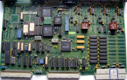
1. It is strictly prohibited to use grounded testing instruments and equipment to test the power amplifier PCB board without an isolation transformer. When coming into contact with equipment with high output power or unfamiliar with the nature of the power supply used, it is necessary to first determine whether the chassis of the machine is live, otherwise it is easy to cause a power short circuit with the live equipment on the chassis, affecting the integrated circuit, and causing the fault to expand. 2. When testing the power amplifier PCB board, attention should be paid to the insulation performance of the electric soldering iron. When testing, it is necessary to confirm that the soldering iron is not live. It is best to ground the shell of the soldering iron, and it is safer to use a low-voltage circuit iron of 6-8V. 3. It is very important to understand the working principle of integrated circuits and their related circuits before testing the power amplifier PCB board. It is
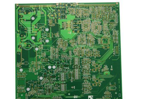
Single panel On basic medical PCB boards, the parts are concentrated on one side, while the wires are concentrated on the other side. Due to the fact that the wires only appear on one side, this type of medical PCB board is referred to as single sided. Due to the many strict restrictions on the design of a single sided circuit board (as it only has one side, the wiring cannot cross and must revolve around a separate path), only early circuits used this type of circuit board. Double-sided board This type of circuit board has wiring on both sides, but if wires are used on both sides, there should be appropriate circuit connections between the two sides. The "bridge" between these circuits is called a through hole. Through holes are small holes filled or covered with metal on medical PCB boards, which can be connected to wires on both sides. Because the area of a double-sided board is twice that of a single panel, it solves the problem of staggered wiring (which can be transmitted
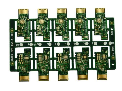
PCBA test stand is a device used to test PCBA finished products. When making PCBA test racks, PCBA processing plants usually need to provide Gerber files and PCBA samples to facilitate the production of test racks. For the current PCBA test bench, only a few pressure plate buckles are installed on the test bench, and the PCBA is fixed by a thimble and pressure plate buckle. During the PCBA function test, press the PCBA into the pressure plate buckle with both hands. Due to uneven force or insufficient compression, PCBA can easily cause poor contact between the testing needle and PCBA, seriously affecting testing efficiency and accuracy; If too much force is applied, it is easy to deform or damage the PCBA when pressing down, and it is also easy to damage the test needle of the testing frame, causing significant losses. 1、 Material preparation After determining the plan based on the information, it is necessary to prepare hardware materials (electronic components), relevant additi
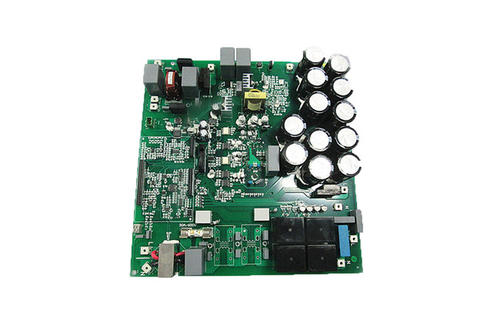
The circuit layout of HDI high-frequency boards is extremely dense, and the production price is slightly higher than that of conventional circuit boards. Only some high-end electronic products will use HDI high-frequency circuit boards, and HDI high-frequency boards include all "blind hole boards" and "buried hole boards". So, what are the differences between identifying blind hole boards and buried hole boards! ① Blind hole: refers to a through hole that connects the inner layer of the PCB to the surface layer of the PCB, but this type of hole does not penetrate the entire board. Buried hole: a through-hole that only connects the wiring between the inner layers, which cannot be seen from the surface of the PCB alone. In this regard, PCB boards with buried blind holes may not necessarily be HDI circuit boards, but HDI high-frequency boards must have blind holes. ② Taking a six layer circuit board as an example: the first/second order refers to PCB boards that require laser drilli
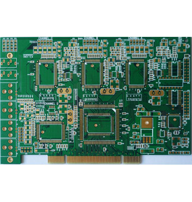
① Hole wall copper thickness: A 25 micron hole wall copper thickness effectively enhances the reliability of PCB boards and improves the Z-axis expansion resistance. ② No welding/patching repair: Perfect for no welding repair and open circuit patching repair, which can effectively ensure the reliability and safety of circuit boards. ③ IPC specifications: For some manufacturers of high-end and high-quality PCB circuit boards, exceeding IPC specifications for cleanliness can not only improve customer satisfaction and trust, but also gain a certain influence in the industry. ④ Service life: Strictly control the surface treatment of each type of PCB circuit board to ensure its solderability and reliability meet industry standards, and reduce the risk of moisture intrusion. ⑤ Substrate: According to the company's positioning standards, select internationally renowned boards to improve product reliability and known performance. ⑥ Ink: Ensure that the solder mask material used compli
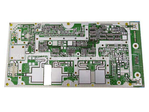
Almost all powered products cannot do without power circuit boards, but due to different application areas, there are differences in customizing power circuit boards in terms of current requirements, product specifications, surface treatment processes, and so on. Firstly, let's understand what types of power supply PCBs include: ① switching power supply ② monitoring power supply ③ high-frequency power supply ④ LED power supply ⑤ production equipment power supply ⑥ digital electronic power supply, etc. For these common power supply circuit boards, the following will explain different types of power supply circuit board products and different process choices. 1. Mobile power circuit boards: These types of circuit boards are usually double-sided or four layer boards, with normal copper thickness, simple circuit design, and surface treatment processes mostly based on tin spraying. 2. Switching power supply circuit boards: Most of these circuit boards are double-sided, with a copper
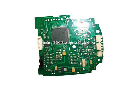
1um=? Mm, 1mil=? The commonly used unit conversion formula for MM circuit board PCB is compiled by Suzhou circuit board sampling manufacturer below. Let's take a look together! For personnel engaged in the PCB industry, it is inevitable to encounter various units of data. Conversion between various units is also frequently needed. It is often necessary to search for conversion values. In order to facilitate the use and learning of PCB practitioners, PCB engineering, PCB electronic engineers, and other personnel. Below are examples of conversion values between various units for your reference. Both Chinese and English abbreviations are indicated. We believe that the unit conversion below is for everyone to keep and learn. Below are examples of conversion values between various units for your reference. Both Chinese and English abbreviations are indicated. We believe that the unit conversion below is for everyone to keep and learn Common units for line width/line spacing/coating th
Inquiry Now

