 +86 755 2794 4155
  sales@knownpcb.com
-
Shenzhen KNOWNPCB Technology Co., Ltd.
 +86 755 2794 4155
  sales@knownpcb.com
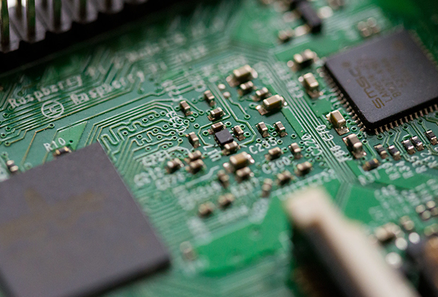
Have you noticed that now more and more of our lighting is using led lighting.What is LED? Compared to the traditional light bulbs, LEDs have lower power consumption, longer lifetime and higher energy efficiency. In the PCB industry,when we say LED PCB, it refers to the pcb used for LED lighting, if you are looking for a suitable LED PCB for your lighting system, this article may bring you something. WHAT ARE LEDS COMPOSED OF?LED is an initial light-emitting diode that produces light when an electric current passes through. LEDs typically have negative and positive electrodes, which generate light in the visible light region.The LEDS are glued to the PCB by soldering process and have electrical connections for lighting.Since light-emitting diodes dissipate a lot of heat when they are in use, when you are designing LED, the metal core is usually the best choice for LED PCB, it is because that it dissipates heat more faster. Among them, the metal material aluminum is the most widely used
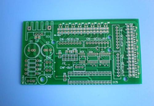
⑴ Differences in longitude and latitude directions cause changes in substrate size; Due to the lack of attention to fiber direction during shearing, shear stress remains in the substrate, and once released, it directly affects the shrinkage of the substrate size. The copper foil on the surface of the substrate is etched off, which limits the variation of the substrate and results in dimensional changes when stress is relieved. When brushing the board, excessive pressure is used, resulting in compressive and tensile stresses that cause deformation of the substrate. The resin in the substrate is not completely cured, resulting in size changes. Especially for multi-layer boards, poor storage conditions before lamination can cause moisture absorption on thin substrates or semi cured sheets, resulting in poor dimensional stability. When the multi-layer board is pressed, excessive glue flow causes deformation of the glass cloth. Solution: ⑴ Determine the variation pattern of longi
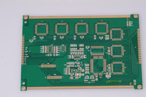
In the manufacturing process of printed circuit boards, there are many processes involved, and each process may have quality defects. These quality issues always involve many aspects, which can be difficult to solve. As the causes of problems are multifaceted, some belong to chemical, mechanical, sheet metal, optical, and other aspects. After decades of production practice, combined with practical experience in solving quality problems and relevant information on solving technical problems, the following summary is made: Defects, causes, and solutions in the manufacturing process of printed circuit boards Solution to the causes of defects in the process There are blisters on the facial mask layer of the film sticking board. The board surface is not clean. Check the wettability of the board surface, that is, the clean surface can keep the water even and the continuous water film lasts for up to 1 minute Low film temperature and pressure increase temperature and pressure The edg
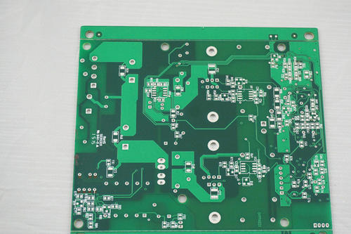
A single panel is on the most basic PCB, with parts concentrated on one side and wires concentrated on the other side. Because wires only appear on one side, we call this type of PCB a single side. Because single panels have many strict limitations in designing circuits (because they are only on one side, wiring cannot cross and must follow separate paths), only early circuits used such boards; The wiring diagram of a single panel is mainly based on screen printing, which means printing a resist on the copper surface, etching it, then marking it with solder mask, and finally completing the part guide hole and shape through punching processing. In addition, some products produced in small quantities are photographed using photosensitive agents to form patterns. Double sided boards have wiring on both sides. However, to use wires on both sides, there must be appropriate circuit connections between the two sides. The bridge between these circuits is called a guide hole (via). A guid
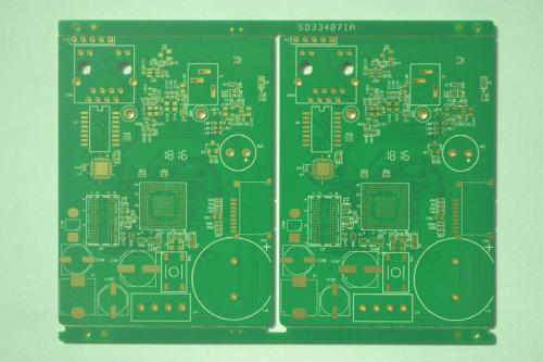
Strictly speaking, PCB double-sided board is a very important type of PCB board in the circuit board. It has a wide range of uses, and it is easy to check whether a PCB board is a double-sided board. I believe that friends can fully grasp the understanding of single panels. Double panels are the extension of single panels, which means that the circuit of single panels is not enough to turn to the opposite side. Another important feature of PCB double-sided boards is that they have conductive holes. Simply put, it means double-sided wiring, with lines on both sides! A summary is: A board with double-sided wiring is a double-sided board! Some friends may ask, for example, if a board has double-sided wiring but only one side has electronic components, is it a double-sided board or a single panel? The answer is obvious, such a board is a double-sided board, only parts are installed on the board of the double-sided board. The advantages of manufacturing PCB double-sided boards are tha
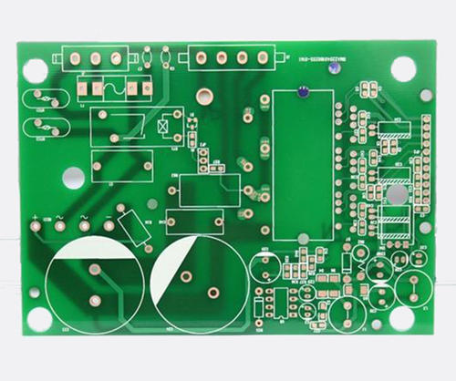
1、 Firstly, considering whether it is a customer design issue, check if there is a connection method between the solder pad and the copper sheet that may cause insufficient heating of the solder pad. 2、 Are there any issues with customer operations. If the welding method is incorrect, it will affect the insufficient heating power, temperature, and contact time. 3、 Improper storage issues. 1. Under normal circumstances, the tin sprayed surface will completely oxidize or even be shorter in about a week 2. The OSP surface treatment process can be stored for about 3 months 3. Long term preservation of sunken gold plates 4、 The issue with flux. 1. Insufficient activity to completely remove oxidation substances from PCB pads or SMD solder joints 2. Insufficient amount of solder paste at the solder joint and poor wetting performance of the flux in the solder paste 3. Part of the solder joints may not be fully filled with solder, which may result in insufficient mixing of the flux
1: The process flow of selective welding includes: flux spraying, circuit board preheating, immersion welding, and drag welding. The flux coating process plays an important role in selective welding. When welding is heated and completed, the flux should have sufficient activity to prevent bridging and oxidation of the circuit board. The flux spraying is carried by an X/Y robotic arm above the flux nozzle on the circuit board, Spray flux onto the soldering position of the double-sided circuit board. 2: The most important aspect of microwave peak selection welding after reflow soldering is accurate flux spraying. Micro hole spraying will never contaminate the area outside the solder joint. Micro point spraying has a minimum flux point pattern diameter greater than 2mm, so the precision of the flux position deposited on the circuit board is ± 0.5mm to ensure that the flux always covers the soldered area. 3: The process characteristics of selective soldering can be understood by comp
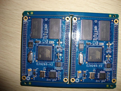
Among them, the most common four layer PCB board thickness in Tongling is 1.6mm, and four layer boards above 3.0mm are relatively rare. Customized 0.6-3.5mm thick PCB boards are supported. The four layer board lamination diagram shows that for a 1.6mm thick PCB, the top layer is 1 ounce of copper, followed by a (0.2mm-0.5oz) thick PP sheet, followed by a second signal layer with a copper foil thickness of only 0.5 ounces, followed by a (1.2mm-0.5OZ) thick core layer, and the bottom layer is a 0.2mm thick PP sheet, Finally, there is a 1 ounce bottom layer. The 6-layer board is similar. PP sheet and core board: Prepregs are thin insulation materials for PCBs. Prepregs, also known as pre impregnated materials, are mainly used as adhesive and insulating materials for the inner conductive patterns of multi-layer printed boards before being laminated. After being laminated, the semi cured epoxy resin is squeezed out, begins to flow and solidify, bonding the multi-layer circuit boards to
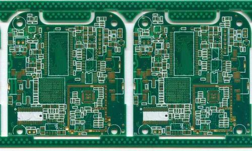
The so-called ceramic circuit board is a type of thermal conductive organic ceramic circuit board prepared using thermal conductive ceramic powder and organic adhesive, with a thermal conductivity coefficient of 9-20W/m.k under conditions below 250 ℃. Ceramic circuit boards are mainly used in areas such as high voltage, high insulation, high frequency, high temperature, high reliability, and small volume electronic products. 1. High precision clock oscillator, voltage controlled oscillator, temperature compensated oscillator ceramic circuit board. 2. Metallization of ceramic substrates for refrigerators. 3. Metallization of ceramic substrates for surface mounted inductors. Metallization of Inductive Magnetic Core Electrodes. 4. High insulation and high voltage ceramic circuit board for power electronic control modules. 5. Ceramic circuit boards for high-temperature circuits in oil wells. 6. Solid state relay ceramic circuit board. 7. DC-DC module power supply ceramic circui
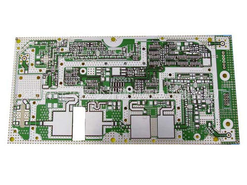
With the continuous updating and upgrading of electronic products, new products have entered thousands of households. However, many friends are not very clear about the production process of PCB sampling factories when they first start planning PCBs, and do not know what line width is more suitable. Below, the editor will based on Professional PCB manufacturers are constantly updating and upgrading their electronic products, and new products have entered millions of households. However, many friends are not very clear about the production process capability of PCB manufacturers when they first plan their PCBs, and do not know what line width is suitable. Below, the editor will provide specific explanations based on the factory's production capability. 1. The width of the primary PCB power line should be above 40 mils, and the width should also be above 25 mils if conditions permit; 2. Other considerations also include practical current. Generally, 10mil can withstand a large curre
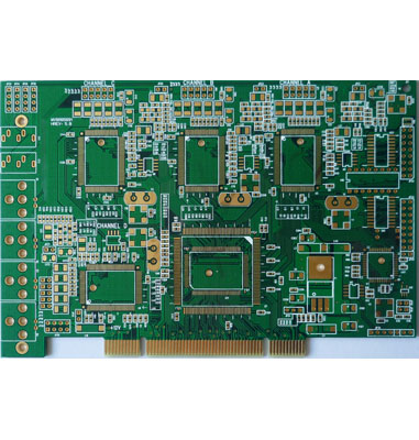
1. Board thickness: 0.8, 1.0, 1.2, 1.6, 2.0 are commonly used standards. If there are no special requirements, choose a board thickness of 1.6mm. 2. Copper foil thickness: 0.5, 1.0, 2.0 are commonly used standards. If the power is not particularly high, it is not necessary to choose a board. Manufacturers usually use a board with a power of 0.5oz. If the power is around 100W, a board with a power of 1.0 or higher will be used. 3. The colors for solder mask: green, black, red, and white are commonly used. If there are no specific requirements, green should be used. If you are using it for your own experiment, green should be used even more, as this color is the clearest for circuit boards. 4. Solder pad treatment: sinking gold, anti oxidation, tin spraying (divided into lead and lead-free), generally using the latter two can be used, and the storage time of tin spraying will be longer. 5. Screen printing colors: White and black are commonly used colors. If it is green oil, white
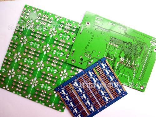
Generally, the thickness of copper foil (covered with copper) for single and double-sided PCB boards is about 35um (1.4mil), while another specification is 50um and 70um. The thickness of the surface layer of the multi-layer board is generally 35um=1oz (1.4mil), and the inner layer is 17.5um (0.7mil). 70% of circuit boards are used to achieve a copper foil thickness of 35um, which mainly depends on the use of the PCB and the size of the signal voltage and current; In addition, for PCBs that require excessive current, some may use 70um copper thickness, 105um copper thickness, and very rarely 140um copper thickness, etc. The thickness of copper foil is usually expressed in oz (ounces), which refers to the thickness of copper uniformly covered by 1oz of copper on an area of 1 square foot, which is approximately 1.4 mils. It is expressed in terms of weight per unit area to indicate the uniform thickness of copper foil. Use a formula to indicate that 1oz=28.35g/FT2 (FT2 is square feet
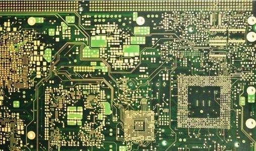
With the continuous updating and replacement of electronic products, from single panel to double-sided board, it can be said that the development is rapid. PCB is known as the "mother of electronic products", and almost all electronic products cannot do without PCB. There are also more and more new products. With the continuous updating and replacement of electronic products, from single panel to double-sided board, it can be said that the development is rapid. PCB is known as the "mother of electronic products", and almost all electronic products cannot do without PCB. There are also more and more new products, and more new products represent There is a constant demand for testing samples, but some cases are quite urgent. When making samples, we will choose urgent ones. So, what is the price of 24-hour urgent PCB sampling? Let me explain in detail below. Common Sense of 24-hour Urgent PCB Sample Prices for Direct Sales by Manufacturers In this era of money, it is the right cho
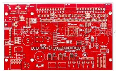
PCB sampling manufacturers generally refer to electronic products being sent to the circuit board manufacturer for processing into circuit boards for inspection after the engineer completes the PCB layout design. Due to being a newly developed product, many functions are still incomplete, and there are still many functional requirements for debugging. Only after debugging is qualified can batch production be carried out. If debugging is not qualified, it is necessary to modify, sample, and debug again, reducing many unnecessary troubles in the later stage. With the increasingly fierce market competition, price issues have become a concern for buyers. The characteristic of PCB sample prices is that they change according to the quantity and delivery time of the samples. Generally speaking, a typical single and double-sided board is not urgent, with a quantity of less than 10 pieces and a standard process within 100 * 100mm. Generally, it only costs 50 yuan. However, if your quantity i
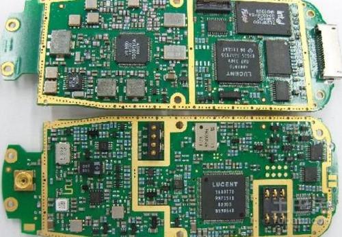
1、 PCB circuit board process elements: 1. Excessive etching of copper foil. The electrolytic copper foil used in the market is generally single-sided galvanized (commonly known as ashing foil) and single-sided copper plating (commonly known as reddening foil). The common copper throwing is generally galvanized copper foil with a thickness of 70um or more, while reddening foil and ashing foil with a thickness of 18um or less have not shown batch copper throwing. 2. During the PCB process, local collisions occurred, causing the copper wire to detach from the substrate due to external mechanical forces. This defect manifests as poor positioning or directionality, with significant twisting of dropped copper wires or scratches/impact marks in the same direction. Peel off the defective copper wire and observe the rough surface of the copper foil. It can be seen that the color of the rough surface of the copper foil is normal, and there will be no side corrosion defects. The peeling stre
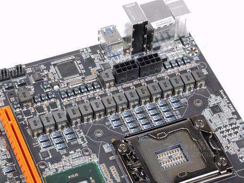
The update and iteration of electronic products are relatively fast, and the development efforts are also increasing. The demand for PCB board making is also gradually growing, and the market share is constantly expanding. With the increasing process requirements and information speed of electronic products, PCB board making is rising rapidly. So, after designing the PCB, what are the relevant parameters and explanations of demand and supply when outsourcing the PCB? Below, the editor will explain them in detail. Relevant parameters and clarification of PCB sample demand and supply 1. Information: The first thing to clarify is what kind of PCB manufacturing materials are required. Currently, the most common one is using FR4, and the main information is epoxy resin peeled fiber cloth board. 2. Board layer: To clarify the number of layers you use to make a PCB. 3. Is it a single piece shipment or a demand for panel shipment? If panel shipment is required, the number of panels nee
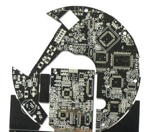
1. The thickness of the board is 0.8, 1.0, 1.2, 1.6, 2.0, which are commonly used specifications. If there are no special requirements, choose a board thickness of 1.6mm. 2. Copper foil thickness: 0.5, 1.0, 2.0 are commonly used specifications. If the power is not particularly high, it is not necessary to choose a board. Manufacturers usually use a board with a power of 0.5oz. If the power is around 100W, a board with a power of 1.0 or above will be used. 3. The colors for solder mask: green, black, red, and white are commonly used. If there are no specific requirements, green should be used. If you are using it for your own experiment, you should use green even more because this color is the clearest for circuit boards. 4. Solder pad treatment: sinking gold, anti oxidation, tin spraying (divided into lead and lead-free), generally choose the latter two, and the preservation time of tin spraying will be longer. 5. Screen printing colors: White and black are commonly used colo
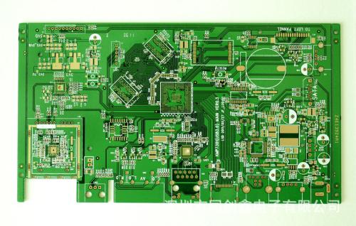
The volume of electronic products is becoming increasingly thin and short, and directly stacking holes on through blind holes is a design method to achieve high-density interconnection. To do a good job of stacking holes, the first step is to ensure the flatness of the hole bottom. There are several production methods, and the electroplating hole filling process is one of the representative ones. Next, let the PCB engineer teach you about the PCB electroplating hole filling process. 1. Advantages of electroplated hole filling: (1) Beneficial for designing stacked holes and holes on the disc; (2) Improving electrical performance helps with high-frequency design; (3) Helps to dissipate heat; (4) Plug holes and electrical interconnections are completed in one step; (5) The blind hole is filled with electroplated copper, which has higher reliability and better conductivity than conductive adhesive. 2. Physical impact parameters The physical parameters that need to be studied in

Dry film is a polymer material that can block electroplating and etching functions. Its reaction principle is to polymerize through ultraviolet radiation, producing stable substances attached to the board surface. It is a widely used consumer material in the microelectronics industry and circuit board manufacturing industry. Today, the editor of CITIC China PCB will talk to you about the types of PCB dry films. 1. Single sided PCB The substrate material is mainly composed of paper phenol copper laminated board (paper phenol as the bottom, covered with copper foil) and paper epoxy resin copper laminated board. Most of them are used in household appliances such as radios, AV appliances, heaters, refrigerators, washing machines, as well as commercial machines such as printers, vending machines, circuit breakers, and electronic components, with the advantage of low prices. 2. Double sided PCB The substrate material is mainly Glass-Epoxy copper laminated board, GlassComposite (glass

In order to save production costs, almost every PCB factory performs panel assembly operations before orders enter the workshop. Splicing boards is not just about putting various small boards together into one big board, but there are many things to pay attention to and important principles. Today, let the editor of Zhongxinhua summarize with everyone~ Firstly, there is the issue of splicing, and the reason for this is to save production costs. To avoid unnecessary waste, splicing treatment will be carried out before production on the circuit board production line without affecting the circuit board. For PCB panel width ≤ 260mm~300mm, it varies depending on the production line. Because we may have many materials and each material gun corresponds to a module in our own processing equipment, if the splicing exceeds the range of the module, the processing speed will become very slow. The outer frame (clamping edge) of the PCB panel should be carefully considered to ensure that the

Rigid flexible combination board is a method of laminating a flexible circuit substrate and a rigid circuit substrate together, which has both the rigidity of a hard board and the flexibility of a soft board. So, what issues should be paid attention to when making rigid flexible composite boards? 1. The design of rigid flexible composite plates usually changes from rigidity to flexibility, and then to rigidity. The rigid region generally has more layers than the flexible region, and the material is transferred from FR-4 to polyimide in the transition region. When intersection occurs, the overlap between rigid and flexible materials needs to keep the holes away from the transition area to maintain integrity. In addition, many rigid and flexible designs incorporate reinforcing materials such as stainless steel or aluminum to provide additional support for connectors and components. 2. Flexible circuits have bent wires that can affect wiring. Due to possible material stress, it is n
Inquiry Now

