 +86 755 2794 4155
  sales@knownpcb.com
-
Shenzhen KNOWNPCB Technology Co., Ltd.
 +86 755 2794 4155
  sales@knownpcb.com
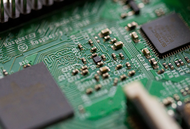
Have you noticed that now more and more of our lighting is using led lighting.What is LED? Compared to the traditional light bulbs, LEDs have lower power consumption, longer lifetime and higher energy efficiency. In the PCB industry,when we say LED PCB, it refers to the pcb used for LED lighting, if you are looking for a suitable LED PCB for your lighting system, this article may bring you something. WHAT ARE LEDS COMPOSED OF?LED is an initial light-emitting diode that produces light when an electric current passes through. LEDs typically have negative and positive electrodes, which generate light in the visible light region.The LEDS are glued to the PCB by soldering process and have electrical connections for lighting.Since light-emitting diodes dissipate a lot of heat when they are in use, when you are designing LED, the metal core is usually the best choice for LED PCB, it is because that it dissipates heat more faster. Among them, the metal material aluminum is the most widely used
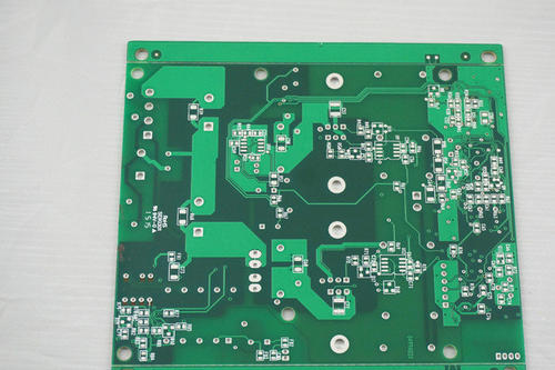
1, engineering production -- light painting machine, film exposure machine 2, opening - opening machine, baking plate oven 3, laminating - brown production line, laminating machine, grinding machine 4, drilling -- CNC drilling machine 5, grinding board -- grinding machine 6, Metallized hole (PTH)-- chemical copper production line (copper wire) 7, graphics transfer - film machine, UV exposure machine or LDI 8, graphic plating - plating production line 9, dry (wet) film - film production line 10, graphic etching ---- etching production line 11, welding resistance layer production -- screen printing machine, UV exposure machine or LDI 12, baking and curing ---- oven, tunnel oven 13, surface treatment --OSP production line or chemical nickel gold line, chemical nickel palladium gold line 14, molding -- punching machine or CNC gong machine, cutting machine 15. Test -- Electric Measuring machine, AOI, 3DAOI. 4, the plate is scratched during the transfer process: a, the ha

1, hot air smoothing (spray tin) Hot air smoothing, also known as hot air solder smoothing (commonly known as spray tin), it is the process of coating molten tin (lead) solder on the surface of the PCB and heating compressed air to smooth (blow), so that it forms a coating layer that is resistant to copper oxidation and can provide good solderability. During hot air conditioning, a copper-tin metal intermetallic compound is formed at the joint of solder and copper. PCB for hot air finishing usually to sink in the molten solder; The air knife blows out the liquid solder before it solidifies; The air knife minimizes the meniscus of solder on the copper surface and prevents solder bridging. 2, organic weldability protectant (OSP) OSP is a process for printed circuit board (PCB) copper foil surface treatment in accordance with the requirements of the RoHS directive. OSP is short for Organic Solderability Preservatives, also known as organic solderability preservatives, also known as
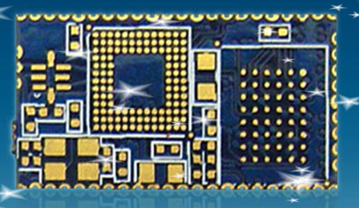
Improvement method: 1, the copper clad plate in the warehouse before IQC must be random inspection, check whether the surface of the board scratches the substrate phenomenon, if there should be timely contact with the supplier, according to the actual situation, make appropriate treatment. 2, the copper clad plate is scratched during the opening process, the main reason is that there are hard objects on the surface of the opening machine, and the friction between the copper clad plate and the objects causes the copper foil scratch to form the phenomenon of exposing the substrate, so the table must be carefully cleaned before the opening of the material to ensure that the table is smooth and there is no hard objects. 3, the copper clad plate is scratched by the drill when drilling, the main reason is that the spindle clip is worn, or the debris in the clip is not clean, the drill is not firmly grasped, the drill does not go to the top, the length of the drill is slightly longer t
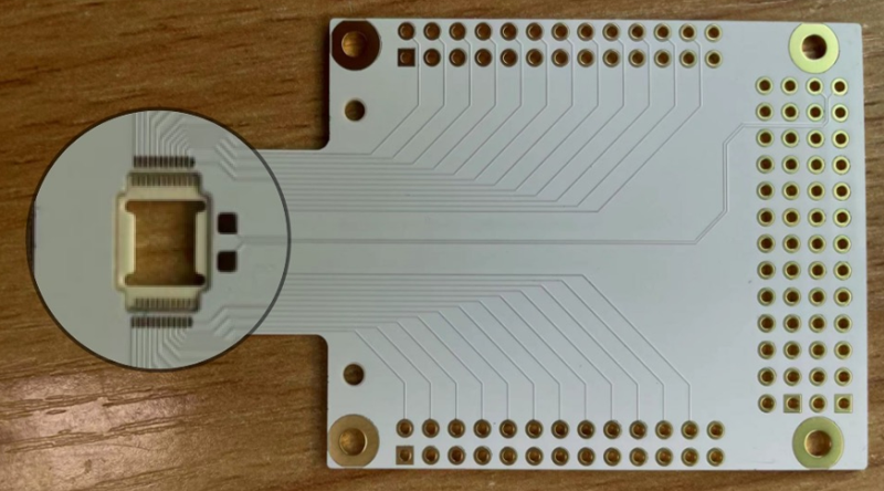
RO4000 Laminates RO4350B Cavity Opening BoardRo4350B material, cavity opening at L1-L2&L6-L5, 4mil bonding pad.Details: Cavity from Top Layer to L2. L2 has exposed pads with ENEPlG Plating for Wire Bonding.Cavity from Bottom Layer to L5. L5 has exposed pads with ENEPIG Plating for Wire Bonding.The 2 cavities are symmetric with each other.
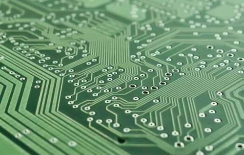
PCB ink is mainly divided into three lines, solder resistance, character ink three categories. The line ink is used as a barrier layer to prevent corrosion of the line, and the line is protected when etched, which is generally liquid sensitive type. There are two kinds of acid corrosion resistance and alkaline corrosion resistance, alkali resistance is more expensive, this layer of ink should be dissolved with alkali after corrosion of the line. Solder resistance ink is applied to the line after the line is done to protect the line. There are liquid photosensitive and heat curing, as well as ultraviolet hardening type, the pad is retained on the board, which is convenient for welding components and plays the role of insulation and oxidation prevention. Character ink is used to mark the surface of the board, such as marking the component symbol, which is generally white. In fact, there are other inks, such as: strippable adhesive ink, which is to protect the part that does not nee
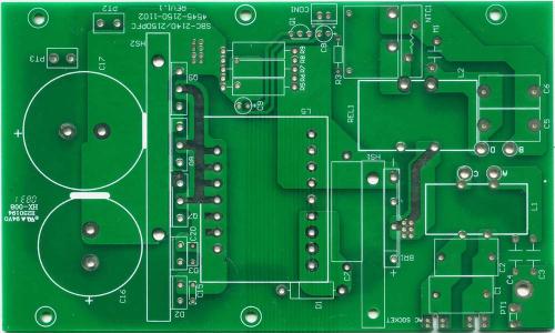
According to the actual experience of the use of ink by most manufacturers, the use of ink must be carried out in accordance with the following provisions: 1, in any case, the temperature of the ink must be kept below 20-25 ° C, the temperature change can not be too large, otherwise it will affect the viscosity of the ink and screen printing quality and effect. Especially when the ink is stored outdoors or at different temperatures, it must be placed at the ambient temperature for a few days or the appropriate operating temperature must be reached in the ink bucket before use. This is because the use of cold ink will cause screen printing failure, causing unnecessary trouble. Therefore, to maintain the quality of the ink, it is best to store or store under normal temperature process conditions. 2, before use, the ink must be fully and carefully manually or mechanically stirred evenly. If the ink enters the air, use it to stand for a period of time. If dilution is required, it is
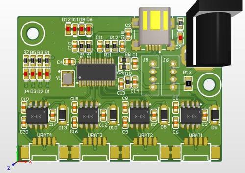
1. Viscosity and thixotropy In the printed circuit board manufacturing process, screen printing is one of the indispensable important processes. In order to obtain the fidelity of image reproduction, the ink must have good viscosity and suitable thixotropy. The so-called viscosity is the internal friction of the liquid, which means that under the action of external forces, one layer of liquid slides on another layer of liquid, and the friction exerted by the inner layer of liquid. The inner layer of the thick liquid has greater mechanical resistance to sliding, and the thinner liquid has less resistance. The unit of viscosity measurement is poisons. In particular, it should be noted that temperature has a significant effect on viscosity. Thixotropy is a physical property of liquid, that is, the viscosity of the liquid decreases in the state of agitation, and quickly recovers its original viscosity after standing. By stirring, the thixotropic effect lasts long enough for its inter
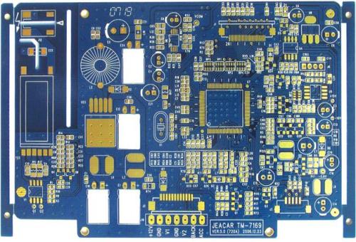
I. The backlight is unstable, and the hole wall is without copper 1. The composition of chemical copper working liquid is out of control or the process conditions are out of control 2. The adjuster is missing or invalid 3. Low activator component or temperature 4. Overspeed 5. Different plates, to drill dirt is too strong 6. The inner layer of the hole wall is broken or peeled off when drilling So how do circuit board manufacturers improve it? 1. The composition and process conditions of the whole working liquid, especially increasing the content of HCHO, appropriately increasing the temperature or reducing the addition of components containing stabilizers, improve the activity of the working liquid. 2. Add or replace the regulator at normal temperature 3. Add activator and increase the temperature 4. Reduce the concentration of accelerant or immersion time 5. Appropriately reduce the decontamination strength, and improve the activity of activator and chemical copper solu

In the process of circuit board manufacturing, what is the copper sinking process of pcb in circuit board factory? And the major circuit board manufacturers are a kind of production process? That's the whole process of sinking copper? Let's take a closer look. In the production process of the circuit board factory, the copper is called plating through the hole, that is, chemical plating copper. In the PCB production process of Shenzhen Circuit Board Factory copper deposition this process requires a chemical reaction, usually abbreviated as PTH, is a self-catalytic REDOX reaction. Generally, double panels or multi-layer boards are sunk after drilling. The role of copper sinking is mainly to connect the circuit, in the non-conductive hole wall substrate, the use of chemical method - chemical copper, because there are electroplated copper behind, copper sinking is to make a base for the copper plating behind, our Shenzhen circuit board factory in the production of PCB process are ve

1. The first step is alkaline oil removal: Alkaline oil removal refers to the removal of oil, finger marks, oxides and dust in the hole; The negative charge of the pore wall is changed into positive charge, which is convenient for the adsorption of colloidal palladium in the later process. Under normal circumstances, oil removal cleaning should be carried out in accordance with the rules of the circuit board factory (Shenzhen circuit board factory is also like this), and the copper backlight test is used for detection. 2. Micro-etching: Micro-corrosion refers to remove the oxide of the plate surface, rough the plate surface, to ensure that the subsequent copper deposition layer and the substrate bottom copper combination; The new copper surface has strong flexibility and can adsorb colloidal palladium very well. 3. Prepreg: The prepreg is mainly to protect the palladium tank from pollution, because the front tank will pollute the palladium tank, and the service life of the pal

The staff of the enterprise often turn a blind eye to many problems, or think that it is harmless, or think that it cannot be changed. There are also many managers who tend to turn a blind eye to intuitive information and focus only on numbers. As a result, it may slip through the cracks, ignore some key clues, and fail to truly understand the true state of the enterprise. As a customer, you should go to the supplier's site to understand its cost composition, production efficiency, quality control. As a supplier, we should go to the customer's site to understand its production process in order to better serve customers. As a peer, if you have the opportunity to visit other circuit board factories, it is also a very good opportunity to learn, compare and reference. Enterprise operation is a big system, all links are closely related and affect each other. For production-oriented enterprises, through any details of the scene, you can know the micro. Any big problem can be found at the

1, PCB wire welding This method does not require any connectors, as long as the external connection point on the PCB printed board is welded directly with the components or other components outside the board. For example, the speaker in the radio, the battery box, etc. Circuit board interconnection welding should pay attention to: (1) The welding pad of the welding wire should be as far as possible on the edge of the PCB printed board, and arranged according to a unified size to facilitate welding and maintenance. (2) In order to improve the mechanical strength of the wire connection and avoid pulling the solder pad or printed wire off due to the pull of the wire, drill holes near the solder joints on the PCB printed board, let the wire pass through the hole from the welded surface of the printed board, and then insert the solder pad hole from the component surface for welding. (3) Arrange or bundle the wire neatly, and fix it with the board through the wire card or other fast

1. Check and remove the debris adhering to the semi-cured sheet; 2. Check the inner plate: and ensure that there is no debris adhering to it; Our operators do a good job in the laminate positioning template (also known as the press template positioning pin) tooling, templates, and buffer paper before the plate. Whether it is a senior circuit board manufacturer or our operator, according to the performance of the semi-cured sheet used, the relevant temperature setting size provisions: Tg<135t, the maximum temperature setting range is 160-185t; Tg>160t, the maximum temperature setting range is 170-205t. The next step is the pressure of lamination: it squeezes the air between the plates and speeds up the flow of resin to fill the space between the shapes. - Generally, the setting of pressure is divided into four stages: ① Pre-pressure section: drive volatiles and residual gases, so that the layer is closely combined. Precompression is the key of lamination. ② Medium pressure se

1, plate: multi-layer board are using Shengyi /KB A-grade copper-clad plate /PP, Sun/Guangxin ink. As a recognized leading enterprise in the copper clad plate industry, Shengyi board products are used in a large number of cutting-edge PCB factories around the world, and multi-layer board guarantees the excellent performance of PCB finished products from the source. 2, hole copper :PCB production has always strictly followed the IPC secondary standard, the thinnest hole copper of the finished product is greater than 20um, beyond the IPC -- level standard! Due to good plating uniformity and strong deep plating ability,PCB dares to ensure smooth and uniform copper plating of the hole and hole wall, and there is no serious uneven copper plating similar to "10 um somewhere, 30 um somewhere" If the user finds the thinnest copper of the finished hole is less than 20um,PCB promises a full refund; 3, line width and line distance: according to the control of 20% of the soil shipment, but t

1, PCB board width ≤260mm(SIEMENS line) or ≤300mm(FUJI line); If automatic dispensing is required, PCB board width × length ≤125 mm×180 mm. 2, PCB board appearance as close as possible to the conventional graphics, it is recommended to use 2*5, 3*3 board, can be assembled according to the thickness of the board; 3. The outer frame of the PCB assembly should adopt a closed-loop design to ensure that the assembly is fixed on the fixture without deformation. 4. The center distance between the small plates is controlled between 75 mm and 145 mm. 5. There can be no large components next to the connection point between the panel shape and the PCB internal small board, small board and small board, and the edge of the components and board should have a space greater than 0.5mm. 6, four positioning holes are opened at the four corners of the outer frame of the plate, plus the Mark point, the aperture is 4mm(±0.01mm); The strength of the hole should be moderate to ensure that it will no
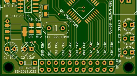
1. Substrate processing problems, for some thinner pcb substrates, due to poor rigidity of the substrate, it is not appropriate to use the brush machine to brush the board, and attention should be paid to control the solid production and processing, so as not to cause the poor bonding force between the substrate copper foil and chemical copper caused by the board bubbling. 2. The surface of the plate in the machining (drilling, laminating, milling, etc.) process caused by oil, or other liquids contaminated with dust pollution surface, will cause the surface foaming phenomenon. 3. The copper brush plate is bad, the grinding plate pressure is too large before copper sinking, resulting in hole deformation, so that the hole foaming phenomenon will be caused in the process of copper plating and tin-spraying welding. 4. Washing problem, due to copper plating to go through a large number of chemical solution treatment, all kinds of acid and alkali inorganic, organic and other drug solv
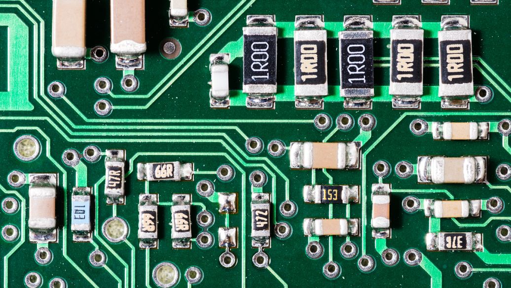
Cutting: According to the requirements of engineering data MI, on the large sheet plate that meets the requirements, cut into small pieces of production plate. Small sheet material that meets customer requirements. Process: Large plate material - cut plate according to MI requirements - curium plate - beer rounded or edging - out of the plate. Pressing: The pressing of the pcb four-layer board needs to go through two operations, first the inner two layers of the board after drilling, and then the outer layer and the inner layer are pressed again. Drilling: According to the engineering data (customer data), drill out the desired aperture at the corresponding position on the sheet material that meets the required size. Process: Stack pin -- top board -- drilling -- bottom board -- inspection/repair. Copper sinking: Copper sinking is the use of chemical methods on the insulation hole wall deposited on a thin layer of copper. Process: rough grinding -- hanging plate -- automatic coppe
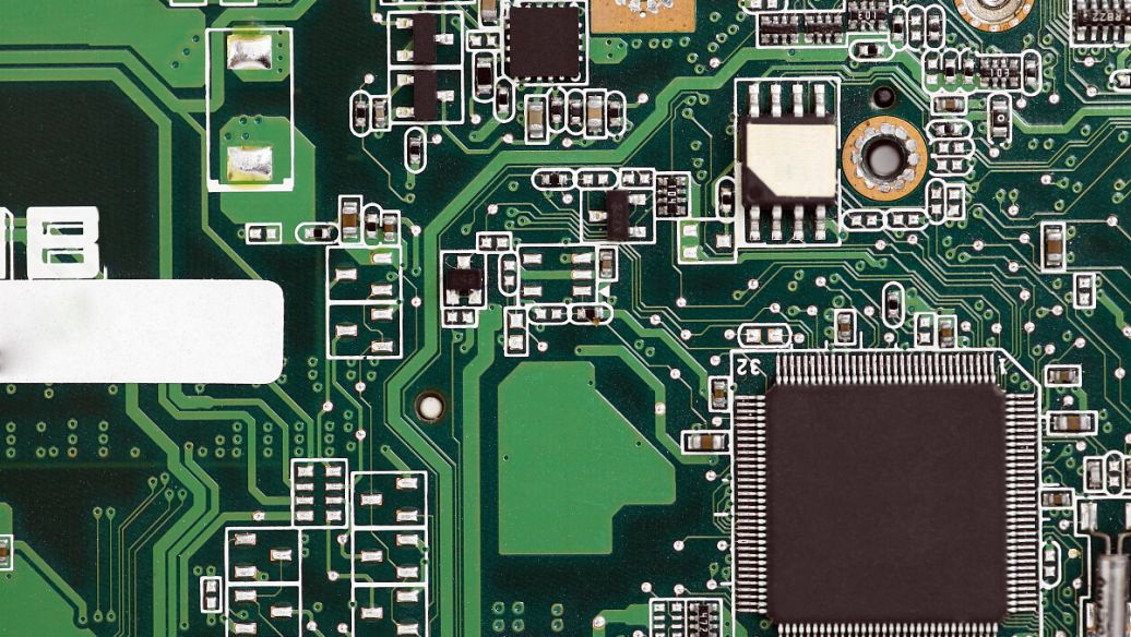
1, the line width is wider than the fine line: because there is a fine line limit in the manufacturing process, the width is not limited. Adjusting the line width to adjust the impedance at a later stage and reach the limit can be cumbersome, which increases the cost or relaxes the impedance control. 2, there is an overall trend: there may be multiple impedance control targets in the design, so the overall size is too large or too small, and there is no need to be out of sync. 3, consider the residual copper rate and glue flow: when one or both sides of the prepreg are etched lines, during the pressing process, the glue will fill the etching gap, so the glue thickness time between the two layers is reduced. If the residual copper rate and glue flow rate are not calculated correctly, and the dielectric coefficient of the new material is not consistent with the nominal value, signal integrity problems may occur. 4, specify the glass cloth and glue content: different glue content o
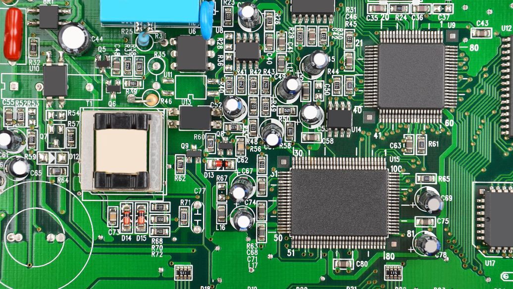
Through hole (VIA), this is a common hole used for conducting or connecting copper foil lines between conductive patterns in different layers of the circuit board. Such as (e.g., blind holes, buried holes), but can not insert the component lead leg or other reinforcement material copper plated holes. Because the PCB is formed by the accumulation of many copper foil layers, each layer of copper foil will be covered with a layer of insulation layer, so that the copper foil layer can not communicate with each other, and the link of its signal depends on the through hole (via), so there is the title of the Chinese through hole. The characteristic is: in order to meet the needs of customers, the through hole of the circuit board must be strengthened, so that in changing the traditional aluminum plug process, the circuit board surface welding and plug hole are completed with white mesh, so that the production is stable, the quality is reliable, and the use is more perfect. The through h
The content of copper sulfate in each analysis in the production is low, originally divided once a week, and now in the case of excessive consumption, it is divided every day, and copper sulfate has decreased every day, originally controlled in 60-80g/L, but just added the day before, and the next day less 6-7G, I wonder why copper sulfate consumption is so large. Subsequently, according to the production volume to follow up, according to the production capacity of each shift is about 30 square meters, about 60 square meters a day, the copper consumption is about 21KG a day, a large slot of copper ball is about 1400KG, according to the production needs to consume 21KG a day, so, according to the theory, the copper ball must be added every week 147KG. After two weeks of observation, the copper ball was not replenished in time in production, and it must be replenished every week, but now it is only replenished once every two weeks. After analysis and observation, it is found that the
Inquiry Now

