 +86 755 2794 4155
  sales@knownpcb.com
-
Shenzhen KNOWNPCB Technology Co., Ltd.
 +86 755 2794 4155
  sales@knownpcb.com
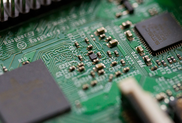
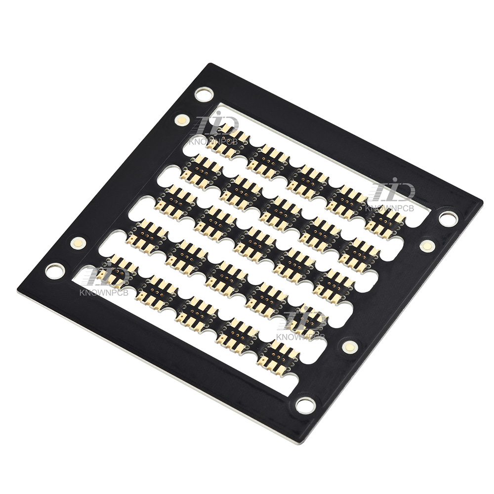
Have you noticed that now more and more of our lighting is using led lighting.What is LED? Compared to the traditional light bulbs, LEDs have lower power consumption, longer lifetime and higher energy efficiency. In the PCB industry,when we say LED PCB, it refers to the pcb used for LED lighting, if you are looking for a suitable LED PCB for your lighting system, this article may bring you something. WHAT ARE LEDS COMPOSED OF?LED is an initial light-emitting diode that produces light when an electric current passes through. LEDs typically have negative and positive electrodes, which generate light in the visible light region.The LEDS are glued to the PCB by soldering process and have electrical connections for lighting.Since light-emitting diodes dissipate a lot of heat when they are in use, when you are designing LED, the metal core is usually the best choice for LED PCB, it is because that it dissipates heat more faster. Among them, the metal material aluminum is the most widely used
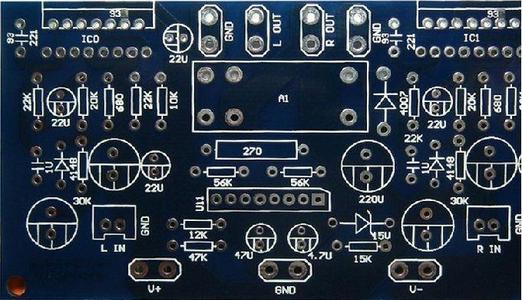
1. The resistance generated by alternating current on components is related to capacitance and inductance. When an electronic signal waveform is transmitted in a conductor, the resistance it experiences is called impedance. 2. Resistance is the resistance generated by direct current on components, which is related to voltage, resistivity, and current. Application of characteristic impedance 1. The electrical performance provided by printed circuit boards for high-speed signal transmission and high-frequency circuits must be able to prevent reflection during signal transmission, maintain signal integrity, reduce transmission losses, and play a matching role. Only in this way can complete, reliable, accurate, worry free, and noise free transmission signals be obtained. 2. The size of impedance cannot be simply understood as better or better, the key is matching. Control parameters of characteristic impedance
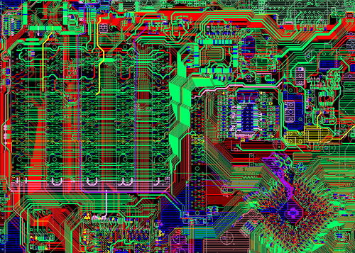
1. Bubbles There are bubbles generated between the lines or on the side of a single line on an FPC printed board after development. Main reasons: The formation of bubbles between two or more lines is mainly due to the narrow spacing between the lines and the high height of the lines. During screen printing, the solder mask cannot be printed on the substrate, resulting in the presence of air or moisture between the solder mask and the substrate. During curing and exposure, the gas expands due to heating, causing a single line to be mainly caused by the high height of the line. When the scraper contacts the line, the line is too high, and the angle between the scraper and the line increases, making it impossible for the solder mask to be printed on the root of the line. This causes gas to exist between the side of the line root and the solder mask layer, and after heating, bubbles are generated. The solution is to visually inspect whether the solder mask is completely printed on the

1. The effect of reducing temperature on the stress of PCB boards Since temperature is the main source of stress on the board, reducing the temperature of the reflow furnace or slowing down the heating and cooling rate of the board in the reflow furnace can greatly reduce the occurrence of bending and warping of the board. However, there may be other side effects, such as solder short circuits. 2. Using high Tg boards Tg is the glass transition temperature, which is the temperature at which a material transitions from a glass state to a rubber state. The lower the Tg value of a material, the faster its board begins to soften after entering the reflow furnace, and the longer it takes to become a soft rubber state, the more severe the deformation of the board. Using a higher Tg board can increase its ability to withstand stress and deformation, but the cost of the material is relatively high. 3. Increase the thickness of the circuit board Many electronic products, in order to ac
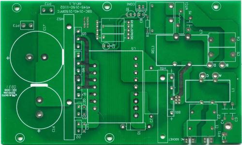
Poor solderability of circuit board holes will result in virtual soldering defects, affecting the parameters of components in the circuit, leading to unstable conduction of multi-layer board components and inner wires, and causing the entire circuit function to fail. The so-called weldability refers to the property of the metal surface being wetted by molten solder, that is, the formation of a relatively uniform and continuous smooth attached film on the metal surface where the solder is located. The main factors affecting the solderability of printed circuit boards are: (1) the composition of the solder and the properties of the soldered material. Solder is an important component of the welding chemical treatment process, which is composed of chemical materials containing flux. The commonly used low melting point eutectic metals are Sn-Pb or Sn-Pb-Ag. The impurity content should be controlled in a certain proportion to prevent the oxide produced by impurities from being dissolve
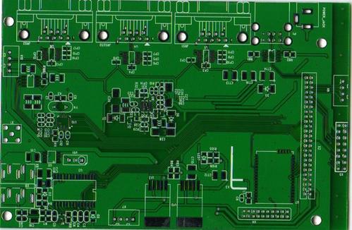
1. Problem: Decreased etching rate in printed circuits Reason: Caused by improper control of process parameters Solution: Inspect and adjust process parameters such as temperature, spray pressure, solution density, pH value, and ammonium chloride content to the specified values according to process requirements. 2. Problem: Deposition of etching solution in printed circuits Reason: (1) The ammonia content is too low (2) Excessive water dilution (3) The specific gravity of the solution is too high Solution: (1) Adjust the pH value to reach the process specified value or appropriately reduce the exhaust volume. (2) Strictly follow the process requirements or reduce the exhaust volume appropriately during adjustment. (3) According to the process requirements, a portion of the solution with high specific gravity is discharged and analyzed, and then an aqueous solution of ammonium chloride and ammonia is added to adjust the specific gravity of the etching solution to the al
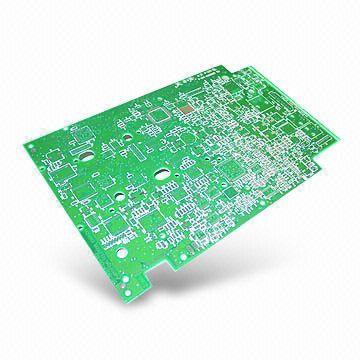
There are certain technical requirements for the rate of copper deposition when using a chemical copper plating solution. If the speed is too slow, it may cause voids or pinholes in the hole wall; If the copper deposition rate is too fast, it will result in rough coating. Therefore, scientific determination of copper deposition rate is one of the means to control the quality of copper deposition. Taking the example of the chemical plating of thin copper provided by Xianling, briefly introduce the method for measuring the copper deposition rate: (1) Material: Using epoxy substrate after copper etching, with a size of 100 x 100 (mm). (2) Measurement steps: A. Bake the sample at 120-140 ℃ for 1 hour, and then weigh W1 (g) using an analytical balance; B. Corrosion in a mixture of 350-370 grams/liter of chromic anhydride and 208-228 milliliters/liter of sulfuric acid (at a temperature of 65 ℃) for 10 minutes, then rinse with clean water; C. Treat the waste liquid from chromium removal
In general, the distribution of copper foil on PCB circuit boards is very complex and difficult to accurately model. Therefore, when modeling, it is necessary to simplify the shape of the wiring and make ANSYS models as close as possible to the actual circuit board. The electronic components on the circuit board can also be simulated using simplified modeling, such as MOS transistors, integrated circuit blocks, etc. Thermal analysis Thermal analysis in SMT processing can assist designers in determining the electrical performance of components on PCB circuit boards, helping them determine whether components or circuit boards will burn out due to high temperatures. Simple thermal analysis only calculates the average temperature of the circuit board, while complex ones require establishing transient models for electronic devices containing multiple circuit boards. The accuracy of thermal analysis ultimately depends on the accuracy of the component power consumption provided by the c
To obtain the accurate cause or mechanism of PCB failure or defect, basic principles and analysis processes must be followed. Otherwise, valuable failure information may be missed, resulting in the inability to continue the analysis or the possibility of obtaining incorrect conclusions. The general basic process is to first determine the failure location and mode based on the failure phenomenon through information collection, functional testing, electrical performance testing, and simple visual inspection, that is, failure localization or fault localization. For simple PCBs or PCBAs, it is easy to determine the location of failure. However, for more complex BGA or MCM packaged devices or substrates, defects are not easy to observe through a microscope and cannot be determined at the moment. In this case, other means need to be used to determine. Next, it is necessary to analyze the failure mechanism, using various physical and chemical methods to analyze the mechanisms that cause

With the development of electronic products towards high density and precision, the same requirements have been put forward for circuit boards. The most effective way to increase PCB density is to reduce the number of through holes and precisely set blind holes and buried holes to achieve this. 1. Definition of blind holes a: Compared to through holes, through holes refer to holes that are drilled through each layer, while blind holes are non drilled through holes. (Illustrated, eight layer board examples: through hole, blind hole, buried hole) b: blind hole subdivision: BLIND HOLE, buried hole Buried HOLE (outer layer not visible); c: Distinguish from the production process: blind holes are drilled before pressing, while through holes are drilled after pressing. 2. Production method A: Diamond belt: (1) : Select reference point: Select a through hole (i.e. a hole in the first drilling strip) as the unit reference hole. (2) Each blind hole drill belt needs to select a hole an
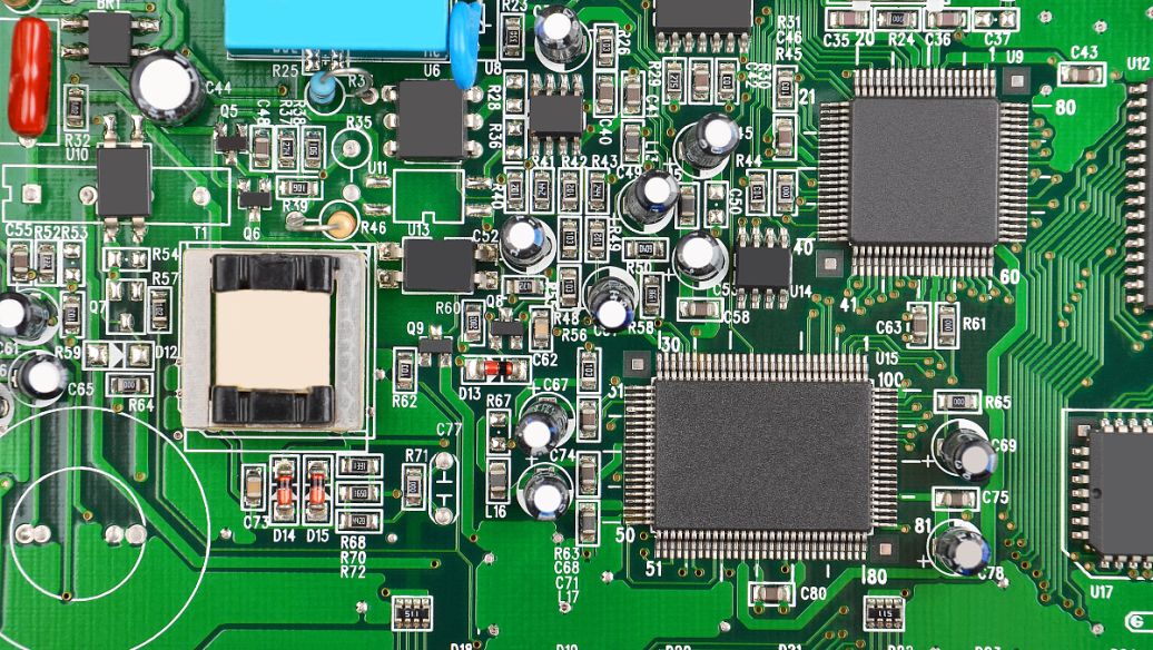
OSP is the abbreviation for Organic Solderability Preservatives, also known as copper protector. Simply put, OSP is a chemical method that grows a layer of organic film on a clean bare copper surface. This film has oxidation resistance, heat resistance, impact resistance, and moisture resistance, used to protect the copper surface of circuit boards from oxidation or vulcanization in normal environments; But in the subsequent welding high temperature, this protective film must be easily removed by the flux quickly, so that the exposed clean copper surface can immediately combine with the molten solder to form a solid solder joint in a very short time. 1. Process flow: degreasing → water washing → micro etching → water washing → acid washing → pure water washing → OSP → pure water washing → drying. 2. Principle: A layer of organic film is formed on the copper surface of the circuit board, firmly protecting the fresh copper surface and preventing oxidation and pollution even at high
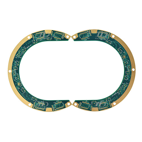
To solve the above problems of gold-plated boards, PCBs using gold-plated boards mainly have the following characteristics: 1. Due to the different crystal structures formed by gold deposition and gold plating, gold deposition will appear more yellow than gold plating, resulting in better customer satisfaction. 2. Due to the different crystal structures formed by sinking gold and plating gold, sinking gold is easier to weld than plating gold, and will not cause welding defects, leading to customer complaints. 3. Due to the fact that only nickel gold is present on the solder pad of the sinking gold plate, the signal transmission in the skin effect is in the copper layer and will not affect the signal. 4. Due to the denser crystal structure of deposited gold compared to gold plating, it is less prone to oxidation. 5. Due to the fact that only nickel gold is present on the solder pad of the sinking gold plate, it will not produce gold wire and cause slight shortening.
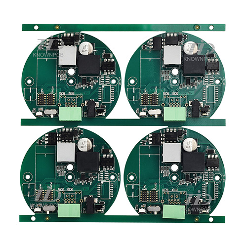
1. Annual maintenance knowledge: 1. Clean the dust on the circuit board. 2. The electrolytic capacitor capacity in the circuit board is randomly checked, if the capacity of the electrolytic capacitor is found to be less than 20% of the nominal capacity, it should be replaced, and the general life of the electrolytic capacitor should be replaced for about ten years to ensure the working performance of the pcb. 3. For high-power devices coated with heat dissipation silicone grease, check whether the heat dissipation silicone grease is dry and solid. For dry and solid devices, remove the dry and solid heat dissipation silicone grease and apply new heat dissipation silicone grease to prevent the high-power devices in the circuit board from burning out due to poor heat dissipation. 2, seasonal maintenance: 1. Clean the dust on the circuit board every quarter, use the circuit board special cleaning solution for cleaning, after cleaning the dust above, dry the circuit board with a ha
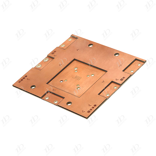
First, the different materials used in flexible circuit boards cause the diversity of prices Taking ordinary double panels as an example, the board material is generally PET, PI, etc., the board thickness ranges from 0.0125mm to 0.10mm, and the copper thickness ranges from 0.0125mm to 0.10mm. Oz to 3 Oz, all of which creates a huge price difference in sheet metal alone; The different brands of materials also have a certain price difference, so the different materials cause the diversity of prices. Second, the different production processes used in flexible circuit boards cause the diversity of prices Different production processes result in different costs. Such as gold-plated plate and tinned plate, the accuracy of the production shape, the use of silk screen lines and dry film lines will form different costs, leading to the diversity of prices. Third, the price diversity caused by the different difficulty of the flexible circuit board itself Even if the material is the same
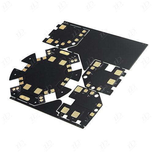
For some customers, pcb sampling production design is seriously non-standard, it is impossible to distinguish which is pad and which is via usage, sometimes conductive holes are processed with pad, sometimes key holes are processed with via, the design is confused, resulting in increased errors, according to incomplete statistics of Jialicom, the problems caused by non-standard design account for more than 50% of customer complaints. And for the current situation of the circuit board, some of the processing of Philin engineers, because the customer design documents are not standardized, and make mistakes, help customers modify the document, the non-standard design, with their own experience to deal with engineering data, which leads to and contributes to the customer's design is not standardized, Jialicang once again stated that the last time you do the right, does not mean that your file is right! All engineers must pay attention to the design standards and specifications! Jialich
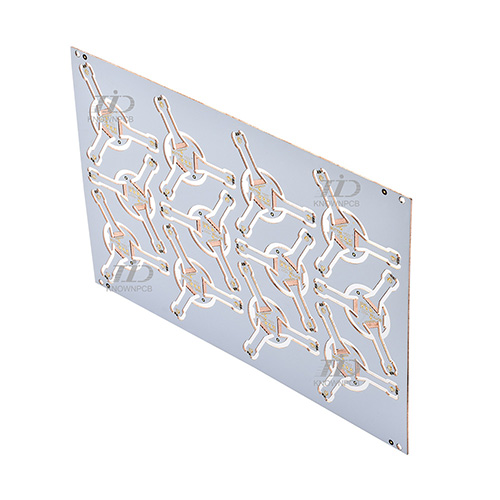
An ordinary pcb board proofing production line needs more than 20 million yuan, multi-layer boards need to invest 50 million yuan, and HDI needs to invest more than 200 million yuan. Due to the huge industry, the division of labor is very fine, there are single-station process outsourcing specializing in drilling, etc., and low-grade products are oversupplied. HDI and other high-end printed circuit board industry is a capital, labor-intensive industry, management and technical requirements are relatively high, often become the bottleneck of capacity expansion. Glass fiber yarn: glass fiber yarn processing by silica sand and other raw materials in the kiln calcined into liquid, through the PCB through the very small alloy nozzle to draw very fine glass fiber, and then hundreds of glass fiber twisted into glass fiber yarn. Kiln construction investment is huge, for the capital intensive industry, 30,000 tons of kiln needs 400 million yuan, the new kiln needs 18 months, the business
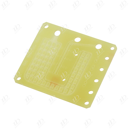
Many customers believe that after a hole is broken, the film temperature and pressure should be increased to enhance its adhesion. However, this view is not correct because the solvent in the corrosion resistant layer evaporates excessively when the temperature and pressure are too high, making the dry film brittle and thin. During development, it is very easy to break the hole. We always need to maintain the toughness of the dry film. Therefore, after a hole is broken, we can improve it from the following points: 1. Reduce film temperature and pressure 2. Improve drilling edge 3. Increase exposure energy 4. Reduce development pressure 5. After applying the film, the parking time should not be too long to avoid causing the semi fluid like drug film at the corner to diffuse and thin under pressure 6. During the film application process, do not tension the dry film too tightly
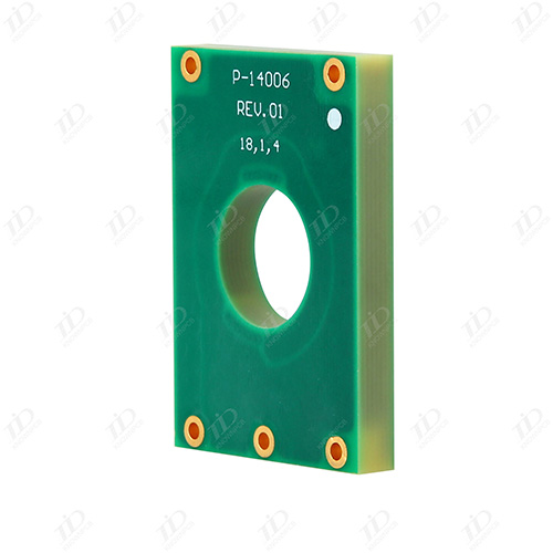
Copper coating, that is, the idle space on the PCB is used as the base level, and then filled with solid copper, these copper areas are also called copper filling. The significance of copper coating is to reduce the ground impedance and improve the anti-interference ability. Reduce voltage drop, improve power efficiency; Also, connect to the ground wire to reduce the area of the loop. If there are many PCB places, such as SGND, AGND, GND, etc., how to cover copper? My approach is that according to the different positions of the PCB board, the most important "ground" is used as a benchmark reference to independently cover copper, and digital and analog copper are separated from each other. At the same time, before coating copper, first bold the corresponding power cable: V5.0V, V3.6V, V3.3V(SD card power supply), and so on. In this way, multiple deformation structures of different shapes are formed. The copper coating needs to deal with several problems: one is the single point con
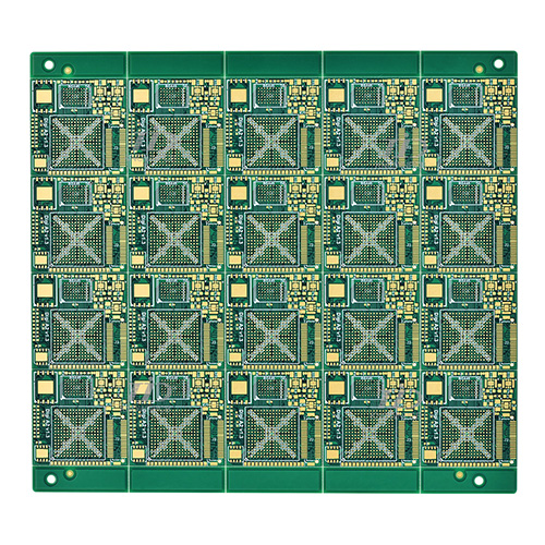
1, 3 points above the line, try to make the line through each point, easy to test, the line length as short as possible. 2, try not to put wires between pins, especially between and around integrated circuit pins. 3, the lines between different layers should not be parallel as far as possible, so as not to form an actual capacitor. 4, the wiring is as straight as possible, or 45 degree line, to avoid electromagnetic radiation. 5, ground wire, power cord at least 10-15mil above (for logic circuit). 6. Try to connect the ground polysemy lines together and increase the ground area. Line to line as neatly as possible. 7, pay attention to the uniform emission of components, so as to install, plug-in, welding operation. The text is discharged in the current character layer, the position is reasonable, pay attention to the orientation, avoid being blocked, easy to produce.
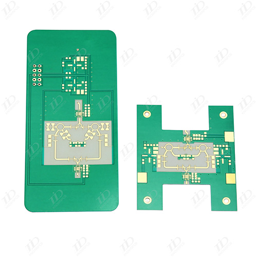
1, choose a reasonable wire width Since the impact interference caused by the transient current on the printed line is mainly caused by the inductive component of the printed wire, the inductance of the printed wire should be minimized. The inductance of the printed wire is proportional to its length and inversely proportional to its width, so a short and fine wire is advantageous for suppressing interference. Signal lines for clock leads, line drivers, or bus drivers often carry large transient currents, and printed wires should be as short as possible. For discrete component circuits, when the width of the printed wire is about 1.5mm, the requirements can be fully met; For integrated circuits, the printed wire width can be selected between 0.2 and 1.0mm. 2, use the correct wiring strategy The use of equal wiring can reduce the inductance of the wire, but the mutual inductance and distributed capacitance between the wires increase, if the layout allows, it is best to use a well
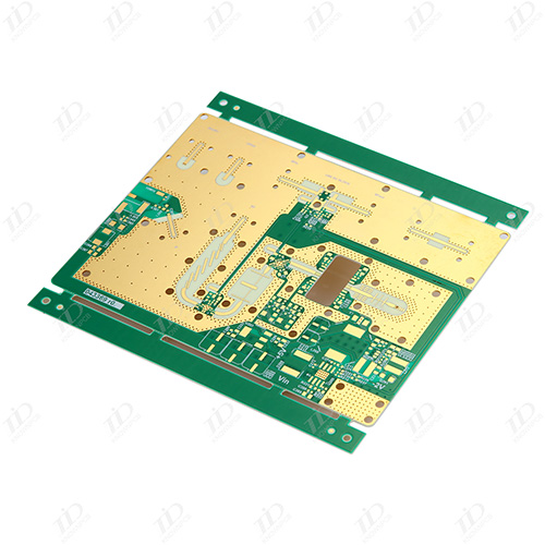
As the carrier of various components and the hub of circuit signal transmission, PCB has become the most important and critical part of electronic information products, and its quality and reliability level determine the quality and reliability of the whole equipment. With the miniaturization of electronic information products and the environmental requirements of lead-free and halogen-free, PCB has also developed in the direction of high density, high Tg and environmental protection. However, due to cost and technical reasons, PCB has a large number of failure problems in the production and application process, and therefore caused a lot of quality disputes. In order to find out the cause of the failure in order to find a solution to the problem and distinguish the responsibility, it is necessary to carry out failure analysis on the failure cases. To obtain the exact cause or mechanism of PCB failure or failure, it is necessary to follow the basic principles and analysis process,
Inquiry Now

