 +86 755 2794 4155
  sales@knownpcb.com
-
Shenzhen KNOWNPCB Technology Co., Ltd.
 +86 755 2794 4155
  sales@knownpcb.com
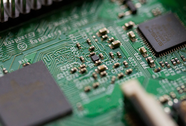
Have you noticed that now more and more of our lighting is using led lighting.What is LED? Compared to the traditional light bulbs, LEDs have lower power consumption, longer lifetime and higher energy efficiency. In the PCB industry,when we say LED PCB, it refers to the pcb used for LED lighting, if you are looking for a suitable LED PCB for your lighting system, this article may bring you something. WHAT ARE LEDS COMPOSED OF?LED is an initial light-emitting diode that produces light when an electric current passes through. LEDs typically have negative and positive electrodes, which generate light in the visible light region.The LEDS are glued to the PCB by soldering process and have electrical connections for lighting.Since light-emitting diodes dissipate a lot of heat when they are in use, when you are designing LED, the metal core is usually the best choice for LED PCB, it is because that it dissipates heat more faster. Among them, the metal material aluminum is the most widely used
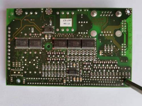
What is a circuit board Printed Circuit Board, commonly known as PCB, is a complex manufacturing process that involves dozens of processes such as inner layer, pressing, and drilling. It is generally classified according to the number of layers and characteristics, and can be divided into three types based on the number of layers: single-layer board, double-layer board, and multi-layer board. Single panel refers to a circuit board where wires are concentrated on one side, Double panel refers to a circuit board with wires distributed on both sides, while multi-layer single refers to a circuit board with more than two sides. Circuit board classification: 1. Flexible board 2. Rigid plate 3. Soft hard combination board Circuit boards can be divided into three main categories based on their characteristics: flexible boards, rigid boards, and soft hard composite boards. Flexible boards, also known as FPCs, are mainly made of flexible substrate materials such as polyester film, whic

1. Design considerations Firstly, before starting the design, it is necessary to understand the copper PCB specified in the design guidelines. From the shared guidelines, it can be understood that it includes considerations such as line width, line spacing, and heat release mode. The increased copper thickness requires wider wiring to accommodate higher currents, and appropriate spacing is crucial for avoiding hot spots and ensuring reliable operation. In addition, selecting suitable materials with excellent mechanical strength and thermal performance is crucial for ensuring robustness. 2. Material selection Careful attention must be paid to the etching process to prevent excessive etching, which may damage the integrity of the copper layer. In addition, the additional weight of copper requires a sturdy substrate to support the structure of the board. You may have a question why industrial power supplies require the use of thick copper plates because they have exceptional heat
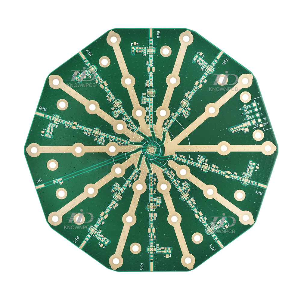
In circuits with resistors, inductors, and capacitors, the resistance to alternating current is called impedance. Impedance is commonly represented by Z, which is a complex number. The real part is called resistance, and the imaginary part is called reactance. The impedance caused by capacitors in a circuit is called capacitance, while the impedance caused by inductors in a circuit is called inductance. The impedance caused by capacitors and inductors in a circuit is collectively called reactance. The unit of impedance is ohms. Impedance type (1) Characteristic impedance In electronic information products such as computers and wireless communication, the energy transmitted in the circuit of a PCB is a square wave signal (pulse) composed of voltage and time, and the resistance it encounters is called characteristic impedance. (2) Differential impedance Two identical signal waveforms with opposite input polarity at the driving end are transmitted by two differential lines, and t
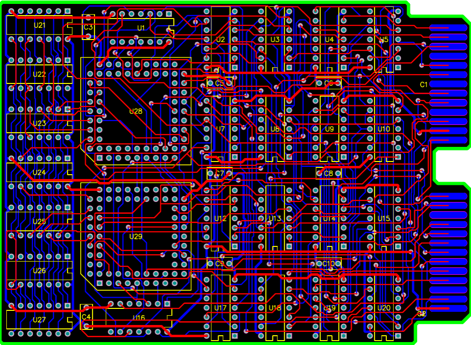
a) Ma Keng: Ma Keng is the result of organic pollution. Large pits usually indicate oil pollution. If the stirring is poor, the bubbles cannot be expelled, which will form pits. Wetting agents can be used to reduce its impact. We usually refer to small pits as pinholes. Poor pre-treatment, metallic impurities, low boric acid content, and low plating temperature can all cause pinholes. Maintenance and process control of the plating solution are crucial, and anti pinhole agents should be used as process stabilizers to supplement. b) Roughness and burrs: Roughness indicates that the solution is dirty, and sufficient filtration can correct it (high pH can easily form hydroxide precipitates, which should be controlled). If the current density is too high, impurities are brought in by impure anode mud and added water, and in severe cases, roughness and burrs will occur. c) Low adhesion: If the copper coating is not fully removed from the oxide layer, the coating will peel off and the adh
Benefiting from the rotational support of terminal new products and new markets, the global PCB market has successfully achieved recovery and growth. According to data from the Hong Kong Circuit Board Association (HKPCA), the global PCB market will develop steadily in 2011, expected to grow by 6-9%, while China is expected to grow by 9-12%. The Taiwan Institute of Industry and Technology (IEK) analysis report predicts that the global PCB output value will increase by 10.36% in 2011, with a scale of 41.615 billion US dollars. According to Prismark's analysis data and the report released by Industrial Securities R&D Center, the changes in PCB application structure and product structure of PCB sampling manufacturers reflect the future development trend of the industry. With the decline in the output value of single/double sided boards and multi-layer boards, as well as the increase in the output value of HDI boards, packaging carrier boards, and soft boards, it indicates that the grow

Single panel Single sided boards are on the most basic PCB, with parts concentrated on one side and wires concentrated on the other side (when there are SMD components, they are on the same side as the wires, and plug-in devices are on the other side). Because wires only appear on one side, this type of PCB is called a single side. Because single panels have many strict restrictions on the design of wiring (as they only have one side, wiring cannot cross and must be routed independently), only early circuits used such boards. Double-sided board Double sided boards have wiring on both sides of the circuit board, but to use wires on both sides, it is necessary to have appropriate circuit connections between the two sides. The "bridge" between these circuits is called a guide hole (via). A guide hole is a small hole filled or coated with metal on a PCB that can be connected to wires on both sides. Because the area of the double-sided board is twice that of a single panel, the doubl
The reason why PCB has been increasingly widely used is because it has many unique advantages, which can be summarized as follows. Can be high-density. For decades, high-density printed circuit boards have developed with the improvement of integrated circuit integration and the advancement of installation technology. High reliability of PCB board sampling. Through a series of inspections, tests, and aging tests, it can be ensured that the PCB can work reliably for a long time (usually 20 years). Designability. The various performance requirements (electrical, physical, chemical, mechanical, etc.) of PCBs can be achieved through design standardization and standardization, with short time and high efficiency. Producibility. By adopting modern management, standardized, scaled, automated production can be carried out to ensure product quality consistency. Testability. We have established a relatively complete testing method, testing standards, various testing equipment and instrum

Entering the PCB prototype factory, the first thing to see is the cutting process, where copper plates of various thicknesses (from 0.4mm to 2.0mm) are cut into appropriate sizes, laying the foundation for circuit board production. This step may seem simple but it is actually very important. If the board size design is not suitable, a lot of edge waste will be generated during the PCB production process. PCB sampling manufacturers will add the price of the waste edge to the customer's board, increasing the unit price. Improving the utilization rate of raw materials as much as possible is an important measure taken by Jiali Chuang to lower the unit price. Then you see the drilling workshop, where the large and small holes on the circuit board are for inserting electronic components or through hole jumpers. This process is completely operated by computer numerical control, and the machine sets the size and coordinates of the through-hole according to the circuit. The accuracy requirem

A multifunctional SMT machine, also known as a high-precision SMT machine or general-purpose machine, can mount high-precision large and irregular components. Generally, it can also mount small chip shaped components, covering almost all component ranges, so it is called a multifunctional SMT machine. Today, let's talk about the basic features of a multifunctional SMT machine: 1、 The structure of functional SMT machines mostly adopts an arch structure, which has the characteristics of high accuracy and good flexibility. 2、 In X and Y positioning systems, full closed-loop servo motors are mostly used for driving, and linear grating encoders are used for direct position feedback to avoid errors caused by screw distortion and deformation. Some use dual electric motors and dual screw rods on both sides of the platform in the y-axis, and use a bilinear grating ruler for feedback, which can effectively reduce the waiting caused by the stationary mounting head and reduce the error cause
To solve the above problems of gilded boards, PCBs using gilded boards mainly have the following characteristics: 1. Due to the different crystal structures formed by depositing gold and gilding, the deposited gold will appear golden yellow and more yellow than gilding, resulting in better customer satisfaction. 2. Due to the different crystal structures formed by sinking gold and gold plating, sinking gold is easier to weld than gold plating, which will not cause poor welding and cause customer complaints. 3. Due to the fact that only nickel gold is present on the solder pad of the sinking gold plate, the signal transmission in the skin effect is not affected by the copper layer. 4. Due to the denser crystal structure of precipitated gold compared to gold plating, it is less prone to oxidation. 5. Due to the fact that only nickel gold is present on the solder pad of the sinking gold plate, it will not produce gold wire causing slight shortness. 6. Due to the fact that only n

As the integration level of ICs increases, PCB sampling manufacturers also have more and more IC pins. The vertical tin spraying process makes it difficult to blow the fine solder pads flat, which brings difficulty to SMT installation; In addition, the shelf life of the tin spray board is very short. And the gilded plate precisely solves these problems: 1. For surface mount processes, especially for 0603 and 0402 ultra small surface mount processes, the flatness of the solder pad directly affects the quality of the solder paste printing process and plays a decisive role in the subsequent reflow welding quality. Therefore, whole plate gilding is often seen in high-density and ultra small surface mount processes. In the trial production stage, the influence of factors such as component procurement is often not that the board is welded immediately upon arrival, but rather that it often needs to wait for several weeks or even months before use. The shelf life of gold-plated boards is l
Single and double-sided PCB circuit boards are the most common and simple PCB boards in the printed circuit board industry. Due to their single panel design and wide circuit design, they are very easy to make. Some simple single panels can be visually inspected without testing costs. During the circuit board quotation process, it was found that there are still a few friends who are not very familiar with the differences between the two, For this reason, I would like to give you a brief introduction on the basic differences between single and double sided circuit boards! What is a PCB single panel: A PCB single panel refers to a circuit board with only one side printed with a circuit, while the other side shows no circuit (note: the other side shows PCB substrate without copper coating); What is a PCB double-sided board: A PCB double-sided board refers to a board that has printed circuits on both sides, and a small number of boards have only one side printed with circuits, while t
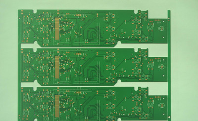
By looking at the cut surface of a PCB board to obtain a four layer board, this method is actually quite difficult, and few people have this kind of vision. However, by observing the guide holes, a four layer board can be identified. If the same guide holes can be found on both sides of the PCB board, or if the motherboard or display card is facing the light source, and the position of the guide holes is not transparent, it is a four layer board. A four layer board is a double-sided board that is then pressed together. During the pressing process, PP and copper foil are added to both sides of the double-sided board, and then subjected to high temperature and pressure to form a multi-layer board. Simply put, the four layer board has an inner layer, and in the process, some circuits are etched through the inner layer, which is then pressed together. The double panel is a board that is directly cut from the incoming board and can be drilled for production. How to draw a four layer bo
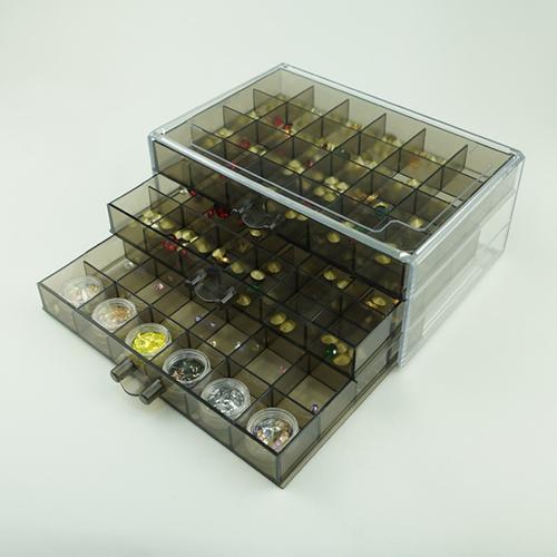
The purpose of equalizing the line length of high-speed digital PCB boards is to maintain the delay difference of each signal within a certain range to ensure the effectiveness of the system in reading data within the same cycle (when the delay difference exceeds one clock cycle, the data). Typically, the delay difference does not exceed 1/4 clock cycles, and the line delay difference per unit length is also fixed. The delay is related to the line width/line length/copper wire thickness and layer structure, However, line length increases the distributed capacitance and inductance, thereby improving signal quality. Therefore, clock IC pins are usually connected to the RC terminal, but serpentine routing does not play an inductive role. On the contrary, inductance will cause higher harmonic phase shifts in the rising component of the signal, leading to a decrease in signal quality. Therefore, it is necessary to maintain the serpentine spacing at least twice the line width, resulting

1: Process factor: a: Copper foil is excessively etched. The electrolytic copper foil used in the market is generally single-sided galvanized (commonly known as ashed foil) and single-sided copper plating (commonly known as reddened foil). The common copper throwing is generally galvanized copper foil above 70um, while reddened foil and ashed foil below 18um have not undergone bulk copper throwing. b: During the production process, there is a local collision, and the copper wire is detached from the substrate due to external mechanical force. This defect is manifested as poor positioning or directionality. The detached copper wire will have obvious twisting or scratches/impact marks in the same direction. When peeling off the defective copper wire, it can be seen that the color of the copper foil surface is normal, and there will be no side corrosion defects. The peeling strength of the copper foil is normal. c: Unreasonable PCB circuit design, using thick copper foil to design o

The new energy charging pile circuit board is different from other consumer electronic products, as the charging pile circuit board needs to meet high current and high voltage during operation, which is generally not withstood by conventional thin plates. Although all PCB boards are made of copper material, there are still certain differences in grade. Ordinary plates are below TG140, while the substrate used to make the new energy charging pile circuit board needs to be above TG150, which is a high TG material, according to the data, The higher the level parameter, the better the quality of the board. The precautions to be taken when customizing a charging station PCB circuit board include: circuit defects, residual copper on the circuit side, and yellow impedance on the hole side are not allowed. For manufacturers of charging station circuit boards, they also need to implement IPC-III standards to prevent products that do not meet the standards from being eliminated in a timely ma
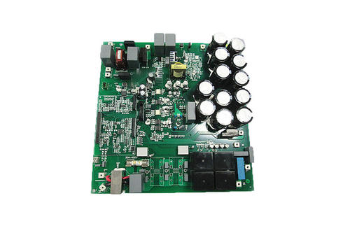
1. Power cord design: Based on the current of the sample circuit board, the power cord should be designed with a thicker width as much as possible, and the loop resistance should be appropriately reduced to ensure that the direction of the power cord and ground wire is consistent with the direction of data transmission. This design helps to enhance noise resistance. 2. Ground wire design: Digital ground and analog ground should be designed separately. If there are both logical and linear circuits on the circuit board, they should be separated as much as possible during design. Even for low-frequency circuits, single point parallel grounding should be used as much as possible. When there are difficulties in actual wiring, partial series connection can be used before parallel connection to ground. High frequency circuit boards should be grounded in series with multiple points, and the grounding wire should be short and leased. Grid shaped large area grounding foil should be used aro
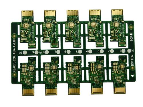
① Dielectric constant: Dk needs to be small and stable. Generally, the smaller Dk, the faster the signal transmission speed, which is inversely proportional to the square root of the dielectric constant of the substrate. The larger Dk, the more likely it is to cause signal transmission delay. ② Dielectric loss: At the same time, the smaller the Dk, the better the signal transmission quality, and the smaller the dielectric loss, the smaller the signal loss. ③ The thermal expansion coefficient of copper foil should be consistent as much as possible, with low water absorption, other heat resistance, chemical resistance, impact strength, peel strength, and other aspects that must be well protected. Normally, high-frequency boards are defined as above 1GHz. Currently, most of the high-frequency circuit board substrates produced are fluorine based dielectric substrates, such as Teflon, which are mostly used for frequencies above 5GHz. Other FR4 substrates are used between 1GHz and 10G
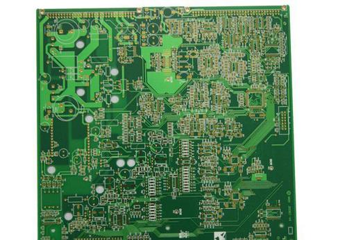
① Benefits: Both high-frequency circuits and low-frequency power supply circuits have voltage gain and output power harvesting effects. Resonant differential amplification circuits refer to the resonant frequency f0, and for fiber optic broadband differential amplification circuits, they refer to a frequency range. ② Pass band: The concept is quite different from that of low-frequency power circuit boards. For resonant differential amplification circuits, most of them are the values between the two corresponding frequencies when the normalized vibration amplitude of the resonance frequency f0 decreases to 0.707; For fiber optic broadband amplification circuits, it refers to the corresponding meaning relative to a certain frequency. ③ Selectivity: Selectivity is mainly aimed at resonant amplification circuits, which characterizes the selection of useful signals and the suppression ability of useless signals in the circuit. It is usually measured using rectangular coefficient and s
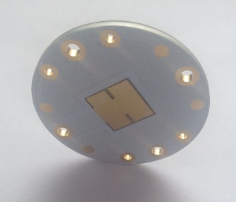
At present, the common colors of PCB circuit boards in the market are green, black, blue, yellow, purple, red, and brown, and recently white and pink PCBs have also appeared. So, why do PCB circuit boards have different colors? Have you noticed that most circuit boards are green, while other colors are rare? Why is this? Next, the editor of the circuit board manufacturer will spread a wave of knowledge about circuit boards to everyone~ In the production of PCB boards, the final surface of the copper layer is smooth and unprotected, whether it is additive or subtractive. Although the chemical properties of copper are not as good as those of aluminum, iron, and magnesium, pure copper is prone to oxidation under water conditions when in contact with oxygen. However, the thickness of the copper layer in PCB circuit boards is very thin, and the oxidized copper can become a poor conductor of electricity, greatly damaging the electrical performance of the entire PCB. In order to preven
Inquiry Now

