 +86 755 2794 4155
  sales@knownpcb.com
-
Shenzhen KNOWNPCB Technology Co., Ltd.
 +86 755 2794 4155
  sales@knownpcb.com
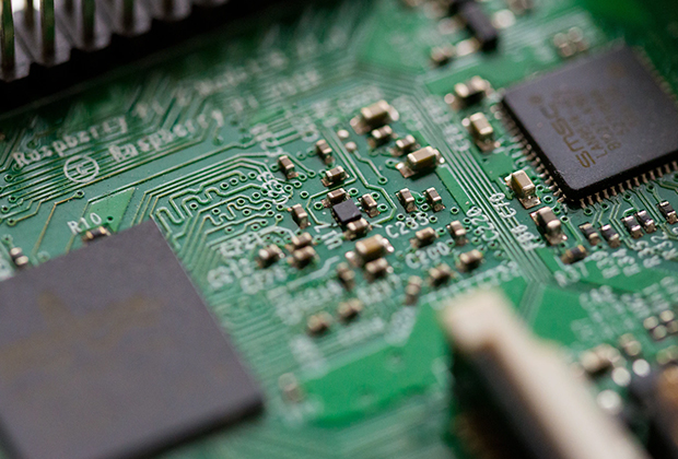
Have you noticed that now more and more of our lighting is using led lighting.What is LED? Compared to the traditional light bulbs, LEDs have lower power consumption, longer lifetime and higher energy efficiency. In the PCB industry,when we say LED PCB, it refers to the pcb used for LED lighting, if you are looking for a suitable LED PCB for your lighting system, this article may bring you something. WHAT ARE LEDS COMPOSED OF?LED is an initial light-emitting diode that produces light when an electric current passes through. LEDs typically have negative and positive electrodes, which generate light in the visible light region.The LEDS are glued to the PCB by soldering process and have electrical connections for lighting.Since light-emitting diodes dissipate a lot of heat when they are in use, when you are designing LED, the metal core is usually the best choice for LED PCB, it is because that it dissipates heat more faster. Among them, the metal material aluminum is the most widely used
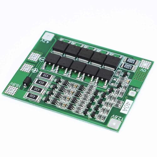
For a PCB sample, please prepare the following information in advance to inquire about it. Being straightforward and not talking nonsense can save you valuable time. More importantly, we are also experts in preparation, and pricing is not at a loss. The PCB circuit board manufacturer has summarized the following points and hopes to help you. Material: What kind of material is required for the design of PCB circuit boards? Currently, FR4 is commonly used, and the commonly used material is epoxy resin peeled fiber cloth board. Board layer: The number of layers for designing PCB circuit boards (the design layers for PCB sampling may vary in price, and the PCB sampling process is similar) Solder resistance color: There are many colors available, which can be selected according to the company's needs, with the commonly used color being green. Screen printing color: The font and border color for screen printing on PCB circuit boards, often selected as white. Copper thickness: Scient
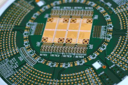
How to check for short circuits on a PCB circuit board? PCB circuit board manufacturers teach you six simple troubleshooting methods. Firstly, computers can easily connect to PCBs, opening up PCB designs, illuminating short-circuit networks, and observing closer areas. Special design should pay attention to internal short circuits in the IC. If it is manual welding, please develop good habits: Before welding, visually inspect the PCB board and use a multimeter to check for short circuits in key circuits (especially power and ground); Welding of finished products for measuring power and ground short circuits using a multimeter to various chips; Do not throw soldering iron randomly during welding. If solder is thrown onto the solder feet of the chip (especially for surface mounted components), it will be difficult to find it. Analyze the main instruments using a short circuit positioning system If there is a BGA processing chip, as all tin points are covered by the processing

Can be high-density For many years, the high-density of printed boards has been able to develop correspondingly with the improvement of integrated circuit integration and the advancement of installation technology. high reliability Through a series of inspection, testing, and aging tests, it is possible to ensure that PCBs can work reliably for a long time (usually with a lifespan of 20 years). Designability The requirements for various properties of PCBs (electrical, physical, chemical, mechanical, etc.) can be achieved through design standardization and standardization. This design has a short time and high efficiency. Producibility PCB adopts modern management, which can achieve standardization, scale (quantity), and automated production, thereby ensuring the consistency of product quality. [2] Testability We have established relatively complete testing methods and standards, which can be used to detect and evaluate the qualification and service life of PCB products thr
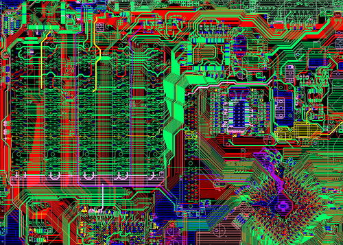
1. Spacing between wires For the processing capacity of Shenzhen PCB manufacturers, the minimum distance between wires should not be less than 3mil. The minimum line distance is also the distance from line to line and from line to pad. From a production perspective, if conditions permit, the larger the better, with a common one being 10mil. 2. Pad aperture and pad width In terms of the processing capacity of PCB manufacturers in Shenzhen, if the pad aperture is mechanically drilled, the minimum should not be less than 0.15mm, and if laser drilling is used, the minimum should not be less than 4mil. The aperture tolerance varies slightly depending on the plate, and can generally be controlled within 0.05mm. The minimum width of the welding pad should not be less than 0.2mm. If copper is laid on a large area, there usually needs to be an internal shrinkage distance of 20mil from the edge of the board. In the PCB design and manufacturing industry, in general, due to mechanical cons
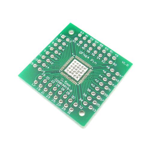
Firstly, a PCB or GERBER file needs to be provided, which should include plate making instructions - including specific requirements such as board layers, materials, solder pad process, ink color, etc. Below, we will provide a detailed explanation of some of the main parameters. Material: It is necessary to explain what kind of material is required for PCB production. Currently, the most common method is to use FR4, which is mainly made of epoxy resin peeled fiber cloth board. Board layer: It is necessary to specify the number of layers for making PCB boards. (The production layers of PCB boards vary, and the price will also vary. The sampling process for PCB circuit boards is very similar.) Solder resistance color: There are many colors available, which can also be selected according to requirements, usually green. Screen printing color: The font and border color for screen printing on a PCB are generally selected as white. Copper thickness: Generally, the scientific calculat
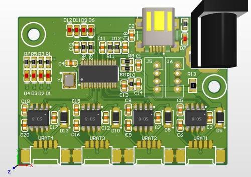
As the name suggests, a multi-layer circuit board can only be called a multi-layer circuit board if it has two or more layers. Previously, we analyzed what a double-sided circuit board is, so a multi-layer board is more than two layers, such as four layers, six layers, eight layers, and so on. Of course, some designs are three or five layer circuits, also known as multi-layer PCB circuit boards. A conductive wiring diagram larger than a two-layer board, with insulating substrates separating the layers. After each layer of wiring is printed, it is then pressed together to overlap each layer of wiring. Afterwards, drilling will be carried out to achieve continuity between each layer of the line through holes. The advantage of multi-layer PCB circuit boards is that the circuits can be distributed and wired within multiple layers, allowing for the design of more precise products. Or smaller products can be achieved through multi-layer boards. Products with larger volumes such as mobile
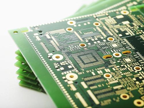
Both sides of the PCB board are copper layers, and PCB boards without resistance welding are prone to oxidation when exposed in the air, resulting in poor product quality and affecting the electrical performance of the PCB board. Therefore, there must be a protective coating on the surface of PCB circuit boards that can block the oxidation reaction between PCB and air, and this coating is a solder mask layer covered with solder mask material. Various colors of solder resist paint have also emerged, forming colorful PCB circuit boards, and solder resist colors have no relationship with the quality and electrical performance of PCB boards. The surface of the PCB board also needs to be soldered with electronic components, so a portion of the copper layer needs to be exposed for easy soldering of components, which is the solder pad. As mentioned earlier, the exposed copper layer is prone to oxidation reaction, so the solder pad also needs to have a protective layer to prevent oxidatio
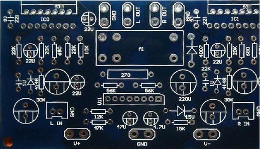
Millimeter wave radar sensors are transitioning layer by layer from 24GHz to 77GHz, and more forward facing and angle radars are considering it appropriate to use the 77GHz scheme. For circuit engineers, selecting the appropriate PCB material is crucial for preset millimeter wave radar. In general, when selecting, it is necessary to consider the selection of thinner PCB circuit board materials, better dielectric constant uniformity, and smaller media damage; At the same time, it is also important to consider the reliable electrical performance and mechanical properties of materials that have reliable external office backgrounds such as time, temperature, and humidity. 8-layer second-order HDI mobile phone board In the preset array receiving antenna of millimeter wave radar, the circuit structure dimensions of different types of channel transmission lines, the phase difference or delay of different channel transmission lines, and the successful implementation of spacing control be
The component library requirements for PCBs are high, which directly affects the installation of the board; SCH's component library requirements are relatively loose, as long as you pay attention to defining pin attributes and corresponding relationships with PCB components. PS: Note the hidden pins in the standard library. After that, the schematic design will be completed, and once it is ready, we will start working on PCB design. Secondly, PCB structure design. In this step, based on the determined circuit board size and various mechanical positioning, draw the PCB board surface in the PCB design environment, and place the required connectors, buttons/switches, screw holes, assembly holes, etc. according to the positioning requirements. And fully consider and determine the wiring area and non wiring area (such as the extent of non wiring area around screw holes). Third: PCB layout. Simply put, layout means placing devices on a board. If all the preparations mentioned earlier are

What is a differential distribution line: A differential distribution line mainly distinguishes the traditional signal transmission method where a signal line corresponds to a ground wire. Differential signal transmission mainly involves signal transmission on both lines, with equal amplitudes and opposite phases of the two signals. Compared to traditional single ended signals, it has advantages such as strong anti-interference, effective suppression of electromagnetic interference, and timing positioning preparation. How to arrange differential lines? When designing circuit boards, two points should be noted for the wiring of differential pairs: Firstly, the length of the two lines should be as long as possible; The other is that the distance between the two lines (determined by the differential impedance) should remain constant, that is, parallel. There are usually two parallel ways, one is for two lines on the PCB board to run on the same side by side layer, and the other

The dielectric constant of a PCB is generally between 4.2 and 4.7 relative to air at room temperature, but this value usually varies with temperature. Generally, its maximum variation can reach 20% in the temperature range of 0 to 70 degrees. The change in dielectric constant will lead to a change in line delay of about 10%, and the higher the temperature, the greater the delay. And it will also change with frequency, the higher the frequency, the smaller the dielectric constant. Different media thicknesses and their different combinations Serial number Theoretical thickness (MM) Theoretical thickness (MIL) Combination method Dielectric constant 1 0.05 1.97 106 * 1 3.9 2 0.07 2.76 1081 * 1 4.2 3 0.08 3.2 LPP1080 * 1 4.2 4 0.1 4 106 * 2 3.9
1) IPC-7525: Template Design Guidelines. Guidelines were provided for the design and manufacturing of solder paste and surface mount adhesive coated templates. Template design using surface mount technology was also discussed, and templates with through-holes or flip chip components were introduced? Kunhe technology, including overprinting, double printing, and stage template design. 2) IPC-Ca-821: General requirements for thermal adhesives. This includes the requirements and testing methods for thermal conductive dielectrics that are used to bond components to suitable locations. 3) IPC-M-I08: Cleaning Instruction Manual. Includes the latest version of IPC cleaning guidance to assist manufacturing engineers in determining the cleaning process and troubleshooting of products. IPC-CH-65-A: Cleaning Guidelines for Printed Circuit Board Assembly Question # e# 4) IPC-7095: Supplement to the design and assembly process of SGA devices. Provide various useful operational information fo
Both sides of a PCB circuit board and above will require copper to be sunk into the holes, making the holes have copper and become electrical holes. However, during the production process, the manufacturer may occasionally discover that there is no copper or copper is unsaturated in the hole after copper deposition. Now, our company briefly describes several reasons. The reason for the absence of copper in the pores is nothing more than: 1. Drill dust plug holes or holes with coarse diameter. 2. When depositing copper, there are bubbles in the solution and no copper is deposited in the hole 3. There is circuit ink inside the hole, no protective layer is applied, and there is no copper in the hole after etching. 4. If the acid and alkali solution in the hole is not cleaned thoroughly after copper deposition or plate electrification, and the parking time is too long, slow bite corrosion will occur. 5. Improper operation and prolonged residence time during micro etching process.
1、 Introduction: With the continuous improvement of human requirements for living environment, the environmental issues involved in the production process of PCB circuit boards are particularly prominent. The topic of lead and bromine is currently the most popular; Lead-free and halogen-free technologies will affect the development of PCB circuit boards in many ways. Although at present, the changes in the surface treatment process of circuit boards are not significant and may seem distant, it should be noted that long-term slow changes will lead to significant changes. With the increasing demand for environmental protection, the surface treatment process of PCB circuit boards is bound to undergo significant changes in the future. 2、 The purpose of surface treatment is to ensure good weldability or electrical performance, which is the most basic purpose of surface treatment. Due to the tendency of copper in nature to exist in the form of oxides in the air, it is unlikely to remai
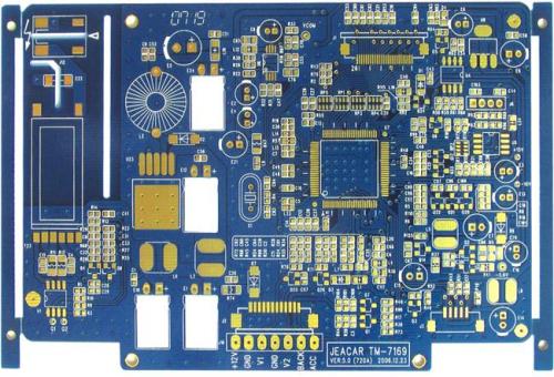
The holes on a circuit board are generally divided into copper holes and non copper holes. Non copper holes are mainly used for positioning and installation, and generally belong to larger holes with a diameter of 0.8mm or more. A through hole usually belongs to a plug-in or via hole, and the most common hole on a PCB board should be a via hole (conduction hole). The aperture of the plug-in hole is larger than the size of the via hole, usually above 0.5, based on the installation of capacitors, resistors, sockets, and other components. The main function of the electric hole is to conduct electricity, and the aperture is generally small, with a common aperture of less than 0.3. With the increase of precision boards, the functional requirements of the product increase, and the number of circuit board layers increases, the aperture is also getting smaller and smaller, with the minimum aperture of 0.1mm. Laser drilling is required. The through-hole needs to have a conductive effect, an
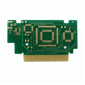
1. The surface of the welding area is contaminated, coated with flux, or metal compounds are generated on the surface of the SMT component. It can cause poor wetting. Sulfides on the surface of silver and oxides on the surface of tin can cause poor wetting. 2. When the residual metal in the solder exceeds 0.005%, the activity of the solder decreases and poor wetting occurs. 3. During wave soldering, there is gas on the surface of the substrate, which can also lead to poor wetting. The methods to solve poor wetting include: 1. Strictly implement the corresponding welding process. 2. PCB circuit boards and component surfaces should be cleaned properly. 3. Select the appropriate solder and set a reasonable welding temperature and time.
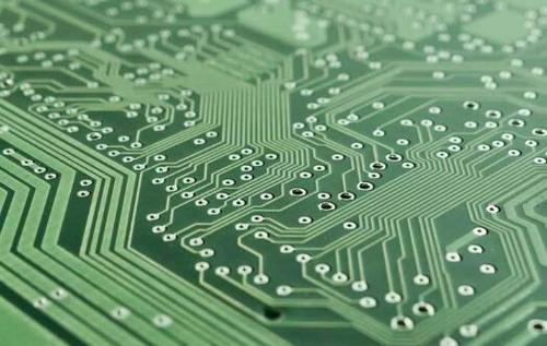
(1) Determine the variation pattern of the longitude and latitude direction and compensate it on the negative film according to the shrinkage rate (this work is carried out before photogrammetry). When cutting at the same time, process according to the fiber direction or according to the character markings provided by the manufacturer on the substrate (usually the vertical direction of the characters is the vertical direction of the substrate). When designing the circuit, it is important to ensure that the entire board surface is evenly distributed as much as possible. If it is not possible, it is necessary to leave a transition section in the space (without affecting the circuit position). This is due to the difference in warp and weft yarn density in the glass fabric structure of the board, resulting in differences in the warp and weft strength of the board. ⑶ Trial brushing should be used to keep the process parameters in a state, and then the rigid plate should be carried out

1. Preparation for welding: Preparation before welding includes cleaning of the welding area, installation of components, and preparation of solder, flux, and tools. Solder wire with the left hand and hold an electric soldering iron with the right hand (keep the soldering iron head clean and keep the soldering head in a welding state at all times). 2. Heating welding parts: Pay attention to heating the entire welding part evenly. 3. Feeding welding wire: After heating the weldment to a certain temperature, the welding wire and soldering iron come into contact with the weldment from the opposite side. 4. Remove the welding wire: When the welding wire melts a certain amount, immediately remove the welding wire. 5. Remove the soldering iron: After the soldering tin has moistened the welding pad or the welding part, remove the soldering iron. Manual soldering of PCB circuit boards is very simple for engineers who often weld them, but for those who have not welded them before, it m
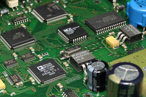
Some people have a strong interest in debugging PCB circuit boards, just like programmers solving bugs. There are many common PCB circuit board problems, including circuit board design, damage to electronic components, circuit shorts, component quality, and PCB circuit board wire breakage. Common PCB board failures mainly focus on components, such as capacitors, resistors, inductors, diodes, triodes, Field-effect transistor, etc. The integrated chips and crystal oscillators are obviously damaged, and the more intuitive way to judge these component failures can be observed through the eyes. There are obvious burning marks on the surface of electronic components with obvious damage. For faults like this, simply replacing the faulty component with a new one can solve the problem. Of course, not all electronic component damage can be observed with the naked eye, such as resistors, capacitors, transistors, etc. In some cases, the damage cannot be seen from the surface and requires the

1. High heating device with heat sink and heat conduction plate When there are a few components in the PCB that have a high heat output (less than 3), a heat sink or heat transfer tube can be added to the heating device. When the temperature cannot be lowered, a heat sink with a fan can be used to enhance the heat dissipation effect. When there are a large number of heating devices (more than 3), a large heat dissipation cover (board) can be used. It is a specialized heat sink customized according to the position and height of the heating devices on the PCB board, or different component high and low positions can be cut out on a large flat heat sink. Snap the heat dissipation cover onto the surface of each component as a whole and dissipate heat by contacting each component. However, due to poor consistency in height during component assembly and welding, the heat dissipation effect is not good. Generally, soft thermal phase change Thermally conductive pad is added on the surface
Inquiry Now

