 +86 755 2794 4155
  sales@knownpcb.com
-
Shenzhen KNOWNPCB Technology Co., Ltd.
 +86 755 2794 4155
  sales@knownpcb.com

Have you noticed that now more and more of our lighting is using led lighting.What is LED? Compared to the traditional light bulbs, LEDs have lower power consumption, longer lifetime and higher energy efficiency. In the PCB industry,when we say LED PCB, it refers to the pcb used for LED lighting, if you are looking for a suitable LED PCB for your lighting system, this article may bring you something. WHAT ARE LEDS COMPOSED OF?LED is an initial light-emitting diode that produces light when an electric current passes through. LEDs typically have negative and positive electrodes, which generate light in the visible light region.The LEDS are glued to the PCB by soldering process and have electrical connections for lighting.Since light-emitting diodes dissipate a lot of heat when they are in use, when you are designing LED, the metal core is usually the best choice for LED PCB, it is because that it dissipates heat more faster. Among them, the metal material aluminum is the most widely used
1. The odd number layer PCB needs to add non -standard layer of core layer bonding process on the basis of the core structure process. Compared with nuclear structures, the production efficiency of the PCB circuit board processing plant with foils outside the nuclear structure will be reduced. Before layer pressing, the outer core needs additional process processing, which will increase the risk of scratching and etching errors. 2. A balanced structure Avoid bending. The best reason for the design without a strange layer of PCB is that the strange layer of the circuit board is easy to bend. After the multi -layer circuit key combination process is completed, when the PCB is cooled, different layer of pressure tension will cause PCB to bend when the core structure and foil structure cool. As the thickness of the circuit board increases, the risk of curvage of two different structures of composite PCB is greater. The key to eliminating circuit boards is to use balanced layers. Altho

1 layer pressure The layer pressure parameters may be different because the plates of different companies may be different. Take the Shengyi substrate and PP as a multi-layer board mentioned above, in order to ensure the full flow of the resin, make the combination of good combination, and require lower the heating rate (1.0-1.5 ° C / min) and multi-paragraph The pressure is coordinated, and the time is required for a long time during the high temperature stage, and 180 ° C is maintained for more than 50 minutes. Here are the recommended sets of boarding program settings and the actual heating of the plate. The binding force of the pressed plate to detect its copper foil and the substrate is 1.ON / MM. The plates after the picture have no layering and bubbles after six thermal shocks. 2 drilling processing Drilling conditions are an important parameter that directly affects the quality of the hole wall of PCB during processing. Because the halogen -free copper plate is used to i

In terms of the principle of halogen -free base boards, most of the halogen -free materials are mainly phosphorus and phosphorus nitrogen. When the phosphorus resin is burned, it is heated to generate polymer phosphoric acid, which is extremely dehydrated. The surface of the high -molecular resin forms a charcoal film. The resin combustion surface contacts the air to extinguish the fire and achieve the flame retardant effect. Polymer resin containing phosphorus nitride compounds produce non -combustible gases during combustion to help the resin system flame retardant. The halogen-free substrate materials are based on the JPCA-ES-01-2003 standard: the copper-covering plate with a chlorine (C1) and bromine (br) content of less than 0.09 % WT, respectively, is defined as a halogen-free copper plate. (At the same time, the total amount of CI+BR ≤0.15 % [1500ppm]). Why do halogen refers to the halogen elements in the chemical element cycle table, including fluoride (F), chlorine (CL),
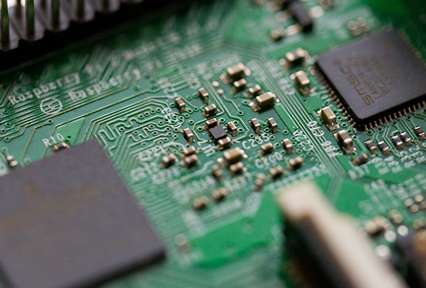
1. Line and Pattern (Pattern): The line is a tool for turning between the original. In the design, the design will be designed as a large copper surface as the ground and power layer. The lines and the diagram are made at the same time. 2. Throughhole/VIA: The guide holes can turn the lines above two levels of lines, and the larger guide holes are used as parts plug -in. Putting and positioning, fixed screws during assembly. Industrial control circuit board 3. SolderResistantant/SolderMask: Not all copper noodles have to eat tin parts, so it will printed a layer of substances from copper noodles (usually epoxy resin) to avoid Non -short circuit between the lines of tin. According to different processes, it is divided into green oil, red oil, and blue oil. 4. Dielectric: It is used to maintain the insulation between lines and layers, commonly known as substrate. 5. Legend/Marking/Silkscreen: This is a non -necessary composition. The main function is to mark the names and positi
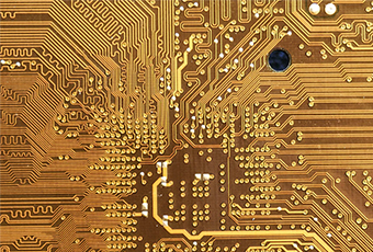
With the continuous expansion of the company's scale, the original company's website has been far from enough...HDI (High Density Interconnect Board) is a compact circuit board designed specifically for small capacity users. Compared to ordinary PCBs, the most significant feature of HDI is its high wiring density, which is mainly reflected in the following four aspects.1、HDI is smaller and lighterThe HDI board is made of the traditional double-sided board as the core board through continuous lamination. This kind of circuit board made by continuous layering is also called build-up multilayer board (Build-up Multilayer, BUM). Compared with traditional circuit boards, HDI circuit boards have the advantages of "light, thin, short, and small".The electrical interconnection between HDI board layers is realized through conductive through holes, buried holes and blind holes. Its structure is different from ordinary multilayer circuit boards. A large number of micro-buried blind holes
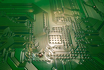
You may always hear about core and prepreg in PCB production. The material is composed of copper foil, reinforcement, resin matrix, and filler system. And each part plays a key role.The appropriate materials have a good quality assurance for the products that produced, but it's not that the more expensive the material is, the more suitable it is for your products.Please kindly contact us KnownPCB, we can provide a variety of material for your better choice.
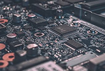
PCB can be called printed circuit board. It is an important electronic component, also a carrier of electronic component, and a provider of electrical connections.Printed Circuit boards are the most active industry in the contemporary electronic component industry, and all electronic products require the use of printed circuit boards. At the same time, they are also used in some electrical products.Advantages of PCBs: minimize and visualize the circuit, it plays an important role in mass production of fixed circuits and optimization of electrical layout.classification of PCBs: 1.By layer:Single sided board, Double sided board and Multilayer board.2.By characteristic: Flex pcb,Rigid pcb , Flex&Rigid pcb.3.By different types of resin:Epoxy resin, Polyester resin, PI resin (polyimide).4.By flame retardant properties : Flame retardant (UL94-VO, UL94-V1), Non-flame retardant (UL94-HB level).Our commonly used materials :SY:S1141/S1000/S1000-2/S1150G/S1170G/S1600L/SH260...KB:KB6160/KB6165/KB6
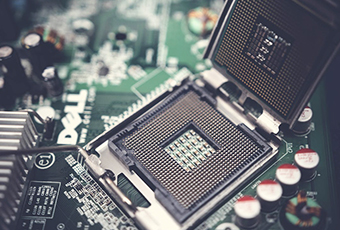
Recently we have produced a new semiconductor board,we would like to share some pictures of our new product as below: The character of this new product as below:1.12 layers with heavy copper 4oz for all layers; 2.The board thickness is 6.35mm; 3.The finishing is ENIG(Au:2u”) + Selectivity hard gold plating (Au:50u”); 4.This board with countersunk and blind routing design; 5.With Via-in-pad design, 6.The aspect ratio is 16:1


Appointment Experience