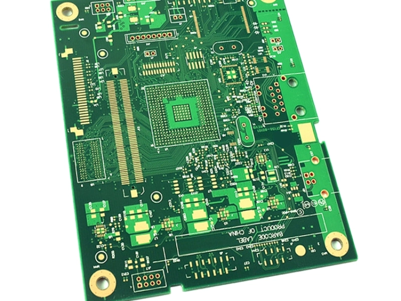
In high-reliability electronics manufacturing, PCB delamination is not merely a cosmetic issue; it is a structural failure mode that can occur during multilayer PCB fabrication or printed circuit assembly manufacturing, compromising signal integrity, thermal stability, and long-term product reliability.
According to the IPC-A-610 standard:
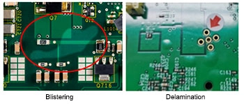
Blistering is a localized swelling caused by separation within laminated base materials, or between the base material and conductive foil or protective coatings.
Delamination refers to the separation between layers of the base material, between the base material and conductive foil, or at other internal PCB interfaces.
Blistering and delamination of printed circuit boards (PCBs) are critical defects that compromise structural integrity and long-term reliability.
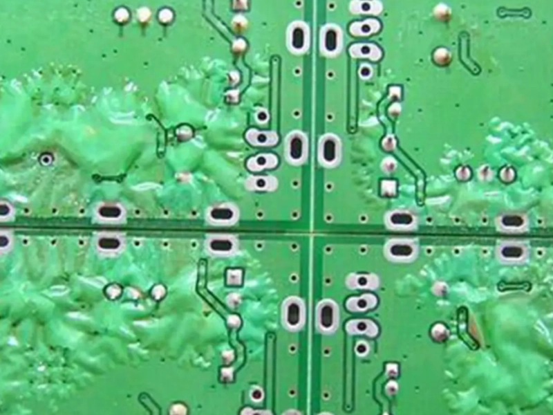
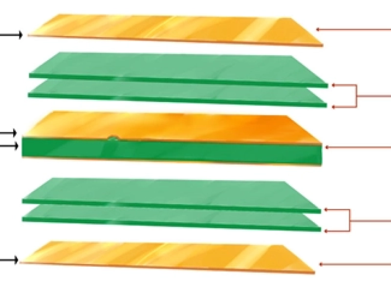
This type occurs at the interface between copper foil and prepreg (PP) resin.
1) Insufficient Adhesion Strength
A small effective contact area between copper foil and resin results in low peel strength, making the interface prone to separation.
2) Excessive Thermal Expansion
During soldering or thermal processing, the base material may expand beyond its tolerance limits. The resulting stress can weaken bonding and cause delamination.
This defect occurs between prepreg layers during lamination.
1) Insufficient Pre-Lamination Dwell Time
Applying full pressure too early causes excessive resin flow. This leads to resin starvation and increases the risk of layer separation.
2) Excessive Pre-Lamination Dwell Time
If full pressure is applied too late, air and volatiles may not be completely evacuated. Trapped voids expand under heat, triggering delamination.
3) Contaminants or Foreign Particles
Impurities interfere with resin polymerization and bonding between PP layers. Under thermal stress, weak interfaces are more likely to separate.
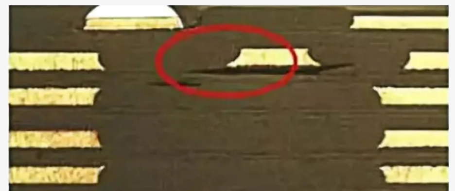
After brown oxide treatment, a uniform organic-metallic layer forms on the copper surface. This microstructure enhances adhesion between copper and PP resin.
If the brown oxide layer is damaged (e.g., scratches or improper surface treatment), bonding strength decreases.
Under thermal expansion stress, the weakened interface becomes susceptible to delamination.
PCB delamination affects electrical integrity, thermal performance, mechanical strength, and long-term reliability. Its impact extends beyond cosmetic defects and can lead to functional failure.
High-speed signal integrity degradation caused by delamination has been discussed in industry publications such as Electronic Design.
When copper traces separate from the dielectric material, several electrical issues may occur:
Increased noise and crosstalk
Impedance variation
Signal reflection
Intermittent open circuits
These changes reduce signal integrity and overall circuit performance, especially in high frequency or high speed designs.
Air has significantly lower thermal conductivity than FR-4 and other laminate materials.
Delamination creates air gaps within the PCB stack-up, increasing thermal resistance. This places additional stress on heat-generating components and may accelerate overheating or thermal fatigue.
Layer separation weakens the structural integrity of the PCB.
The board becomes more vulnerable to:
Mechanical shock
Vibration
Bending stress
This increases the likelihood of cracking, trace breakage, and field failures.
Electrical instability, thermal stress, and mechanical weakening collectively shorten the operational lifespan of the PCB. Reliability decreases over time, particularly in harsh environments.
Delaminated areas make it difficult to form reliable solder joints during maintenance or rework.
In many cases, the separated section must be removed before repair, increasing labor complexity and risk of further damage.
If detected during production, affected boards must be reworked or scrapped, resulting in direct financial loss.
If undetected, field failures can lead to:
Warranty claims
Product recalls
Reputation damage
Delamination can complicate troubleshooting.
Electrical anomalies caused by layer separation may obscure the root cause of failure, leading to longer diagnostic time and increased downtime.
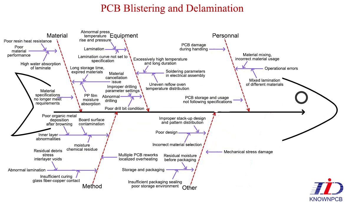
Effective prevention requires coordinated control across design, materials, manufacturing, and assembly.
Maintain balanced copper distribution
Avoid sharp trace corners
Ensure proper spacing
Integrate thermal management features
Good design minimizes internal stress and uneven thermal expansion.
Choose laminate materials with:
Low moisture absorption
High glass transition temperature (Tg)
Strong peel strength
Adequate thermal cycling performance
Material quality directly impacts long-term bonding reliability.
Strictly manage:
Surface preparation quality
Lamination pressure timing
Temperature profile
Resin flow control
Prevent resin starvation, void formation, and weak bonding interfaces.
Moisture is one of the most common causes of PCB delamination.
Pre-bake PCB substrates before assembly to remove absorbed moisture
Store laminates and finished boards in low-humidity environments
Avoid prolonged exposure to uncontrolled storage conditions
Reducing internal moisture minimizes vapor expansion during reflow.
Operate within recommended thermal profiles.
Excessive heating or rapid temperature ramp-up can induce severe expansion stress and trigger delamination.
Implement:
Visual inspection
AOI
Cross-section analysis
Reliability testing
When delamination occurs, conduct root cause analysis and document corrective actions to prevent recurrence.
PCB delamination is a structural reliability defect that affects electrical performance, thermal management, and mechanical integrity.
It is typically caused by:
Moisture absorption
Weak adhesion
Improper lamination parameters
Thermal expansion stress
Surface treatment damage
Through optimized design, proper material selection, strict lamination control, moisture management, and disciplined assembly practices, manufacturers can significantly reduce delamination risk and enhance long term PCB reliability.
In high performance and high reliability applications, preventing delamination is essential to ensure product stability, durability, and brand credibility.
Request for a tech support
 | Download our design guidesfor better PCB designing and manufacturing These are some of the design guides designers and engineersdownload the most:
|
Proven by 7 industries, 4000+ customer projects
Please contact us at sales@knownpcb.com, ask for engineering support here or use the form below to reach out to KnownPCB | Get In Touch Today |