Q
Is placing vias on solder pads a "brilliant idea" or a "bad idea"?
A
In PCB design , vias and pads are two fundamental elements, but their relationship often causes headaches for engineers . Some engineers place vias on pads to save space , only to encounter setbacks during SMT production; others strictly adhere to traditional designs, only to be cornered by the routing constraints of BGA packages . Today, we'll delve into all aspects of vias and pads to help you avoid these design pitfalls.
To understand via pads of PCB, you first need to distinguish between two concepts: via and pad.
Vias are mainly used to connect wires on different layers of the same network . They are generally not used as soldering components. The aperture is usually small, and the surface can be coated with solder resist ink or not.
Solder pads are divided into lead pads and surface mount pads . Lead pads have solder holes and are mainly used for soldering leaded components; while surface mount pads do not have solder holes and are mainly used for soldering surface mount components.
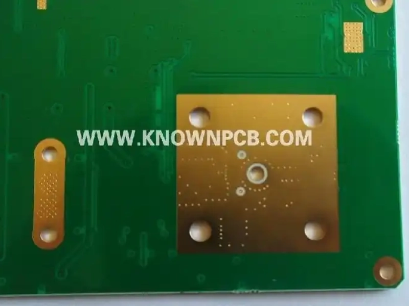
A via pad , simply put, is the ring-shaped copper ring that comes with the via itself . It is part of the via structure and is used to connect circuits.
There are two main reasons for the existence of via pads:
1. Electrical connection function
Vias are needed to transmit signals between different layers , and pads provide reliable connection points.
2. Process Requirements
In PCB manufacturing, vias require drilling and copper plating processes, and solder pads ensure the feasibility of these processes. The minimum width of the solder ring for a via is generally 0.15mm to ensure reliable copper plating.
However, as electronic products become thinner and more multifunctional, PCB design space is becoming increasingly limited, and a special phenomenon has become common— through-pad holes, where vias are directly placed on the pads .
Hole in the dish: A design made out of necessity
The conventional design involves drilling a via next to the pad to connect to the traces on other layers. However, when designing a lot of routing and placing many components , either the PCB board needs to be designed to be very large, or the via needs to be placed on the component pad.
For BGA packaged devices, there is almost no space to place vias next to the small-pitch BGA pads , so in-pad vias become the only option.
While via pads solve the space problem, they may introduce a series of production risks:
1. SMT soldering issues
Solder paste loss: Due to capillary action, solder paste can flow into through-holes, resulting in insufficient solder at the solder joints, leading to cold solder joints or false solder joints.
Air bubbles/voids: When solder paste is printed on through holes, air is trapped inside the holes. During reflow soldering, the air expands due to heat, forming voids in the solder balls. In severe cases, this can even lead to the pillow effect.
2. Limitations of different processing techniques
Via capping: This only covers the surface of the pad, leaving the hole hollow. Under high temperatures, the ink may flow away, causing the "hole opening to turn yellow".
Through-hole plugging: Although it can seal the hole, there is no copper surface to fill the plugged area, reducing the welding area and still posing a risk of weak welding.
3. Appearance and reliability issues
When improper handling methods are used, a phenomenon of "a green dot in the middle of a white solder pad" may occur, which seriously affects the soldering quality and reliability .
To ensure welding quality, for designs that require in-disk holes, the industry recommends resin plugging + electroplating capping.
1. Advantages of the process
Preventing solder leakage: The resin fills the holes, preventing solder paste from leaking out during SMT soldering.
Ensure welding area: After electroplating the cap, the solder pads are flat, providing sufficient area for welding.
Improve reliability: Avoid quality problems such as poor soldering and false soldering.
2. Precautions
This process will increase the copper thickness on the PCB surface (base copper + electroplated copper thickness), which may reach about 60um. Therefore, sufficient margin needs to be left in the design of the line width spacing, and it is recommended not to be less than 4/4mil .
For BGA packaged PCB designs, there are stricter requirements for via pads.
1. Traditional BGA design
Through-hole diameter : ≥0.15mm.
Through-hole copper foil diameter : ≥0.25mm.
BGA pad diameter : ≥0.25mm.
Spacing between drill holes and BGA pads : Minimum spacing requirements must be met.
2. Advanced BGA design
Filling vias with epoxy or copper paste allows for more precise wiring, easily handling BGAs with a 0.5mm pitch.
Design engineers need to pay special attention to the following points when designing via pads:
1. Clarify requirements: Is it really necessary to drill holes in the pads? Can this be avoided by optimizing the layout?
2. Evaluate the process: If a through-hole is required, has the correct POFV process been selected?
3. Check the design: Does the design rule meet the capabilities of the PCB manufacturer?
4. Verify manufacturability: Conduct a comprehensive manufacturability analysis ( DFM ) before board production.
Discovering via pad issues during the design phase saves significant costs and time compared to the production phase. KnownPCB DFM , offer a free PCB manufacturability analysis , helps engineers identify or resolve all potential quality issues early in the manufacturing process, minimizing product development iterations.
KnownPCB DFM's powerful capabilities in via pad inspection:
1. Pad on-hole detection: KnownPCB can detect vias on surface mount pads, identify whether there is a via design in the pad, and provide process suggestions.
2. Drilling analysis: This includes checking the borehole diameter, analyzing the hole-to-hole spacing, and checking the distance from the hole to the board edge, to ensure that the via design meets the production process requirements.
3. Solder mask analysis: Check whether the solder mask bridge is intact and whether the solder mask opening is appropriate to avoid the risk of short circuit due to solder bridging.
4. Circuit analysis: Check if the size of the via ring is sufficient to avoid the risk of open circuit; check the SMD spacing to prevent short circuits caused by solder bridging.
5. DFM analysis: Quickly generate comprehensive manufacturability analysis reports, pointing out potential problems in the design, including via pad related issues.
1. Minimum line width/spacing check: Ensure the design meets manufacturing process requirements.
2. Check pads on characters: Avoid characters covering pads and affecting soldering.
3. Simulation drawing file output: Visually check whether the silkscreen and reference numerals overlap or are obscured.
4. Price and delivery time assessment: Evaluate PCB manufacturing costs and cycle time based on design complexity.
Although via pads are small, they are crucial to the success or failure of the entire PCB project. Understanding the nature of via pads, mastering the correct handling of vias within the pads, and using professional DFM tools for inspection are essential courses for every excellent hardware engineer.
Whether you are a newbie or a seasoned veteran, KnownPCB DFM can be a powerful assistant in your design process , helping you to discover design problems such as vias and pads in advance, so that PCB designs can be approved on the first try and products can be launched to the market faster!
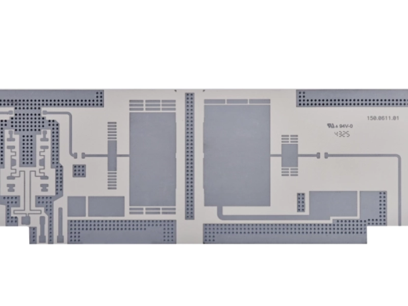
November/12/2025High-frequency Bare PCB | Industrial PCB Manufacturing
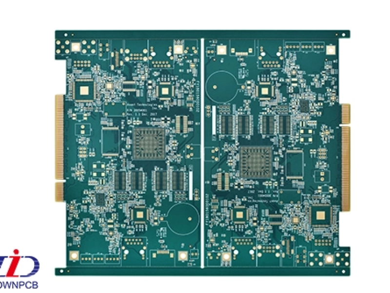
April/20/20268-layer HDI PCB with Edge Connector

March/17/2026Heavy Copper PCB with Complex Shape Machining for High-Current Applications
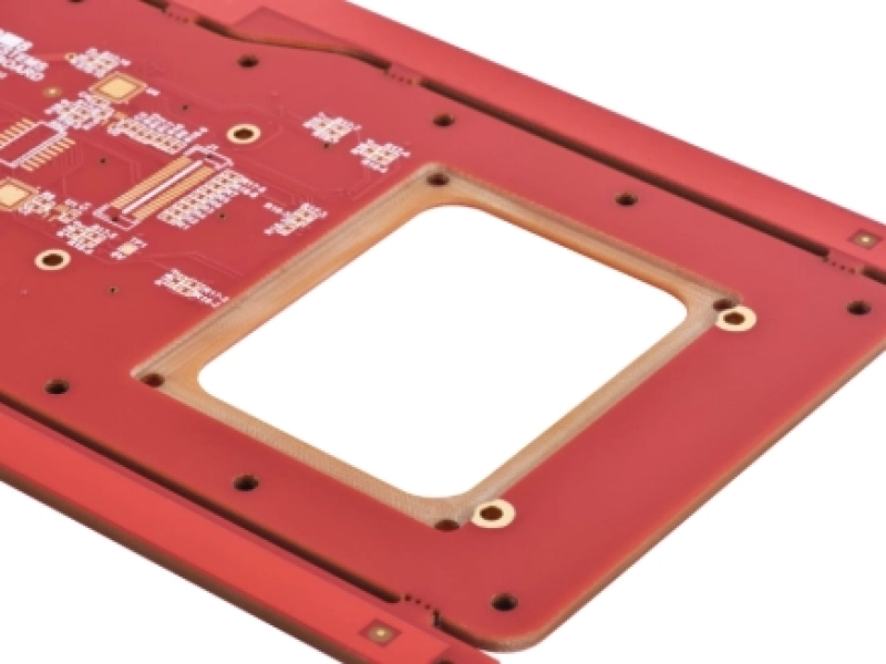
April/21/20268-Layer BGA PCB with VIPPO technology
March/25/2026Industrial Control PCB with Hard Gold 15U
