Get A Quote
CN
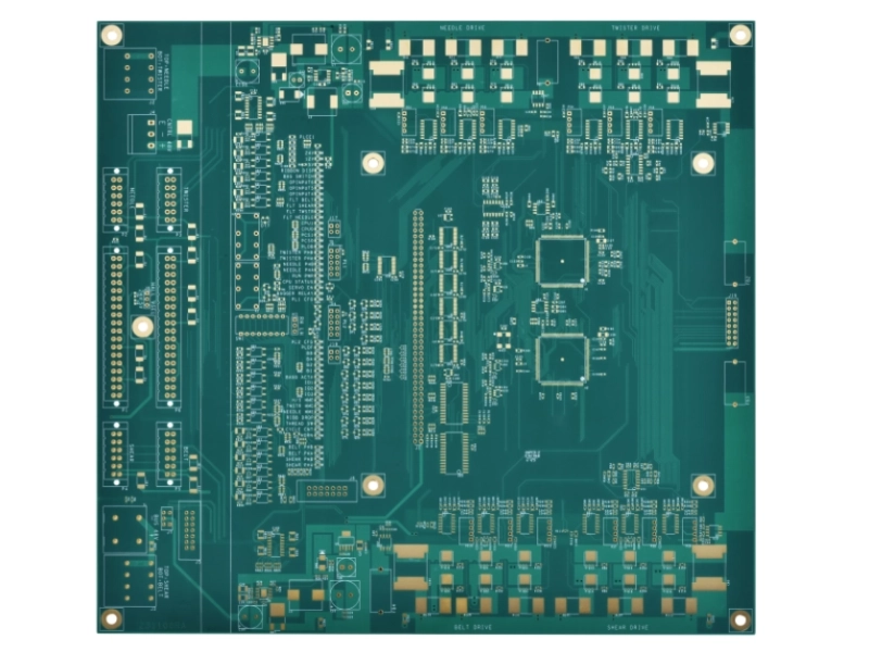
This is a high-density BGA PCB project that previously completed by KnownPCB.
This 4-layer board includes multi-unit panel layout, multiple fine-pitch BGA pads, and features ENIG (Electroless Nickel Immersion Gold) as surface finish.
Therefore, for this high-density PCB design with BGA pads, the core manufacturing challenge is to control the precision and consistency of fine-pitch BGA pad areas, and ensure the soldering stability for mass SMT assembly.
Manufacturing parameters of High-density PCB panel with fine-pitch BAG pads:
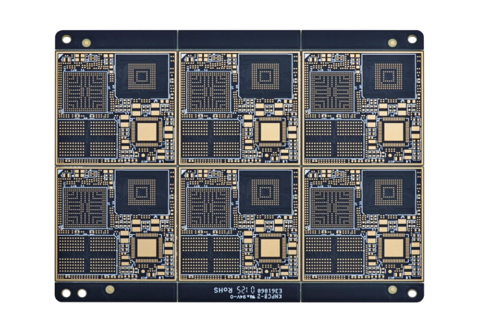 |
Base Material |
FR4 |
|
Layers |
4 |
|
|
Dimensions |
92*72 |
|
|
PCB Thickness |
1.6 mm |
|
|
Board Solder Mask Color |
Black |
|
|
Silkscreen |
White |
|
|
Surface Finish |
ENIG 2U" |
|
|
Material Type |
FR4 TG135 |
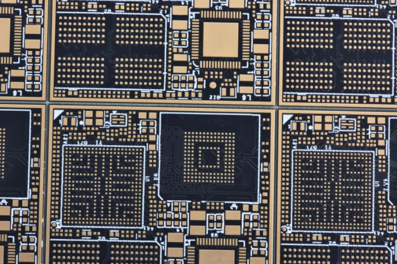
The final soldering result of high-density board is directly determined by the quality of its BGA pads, since BGA solder joints are placed underneath the chip and can not be checked visually after assembly.
Therefore, for this fine-pitch BGA PCBs, the critical manufacturing challenges are mainly concentrated on the BGA pad areas. Solving these problems can ensure BGA pad consistency and stable production.
1. Tolerance deviations in BGA pad size will impact the performance of solder ball wetting and soldering uniformity.
2. Solder mask opening offset can increase the risk of BGA solder bridging and insufficient copper exposure.
3. The flatness and uniformity of ENIG surface finish will affect the quality and reliability of BGA solder joints.
In the conclusion, the key manufacturing point of this high-density PCB is not only about the fabrication of individual BGA pads, but about the sustaining consistent pad size, solder mask opening and ENIG surface uniformity over the whole high-density board panel.
To solve these three manufacturing difficulties, KnownPCB have implemented the following process controls.
Firstly, KnowenPCB ensured stable BGA pad dimensions through engineering compensation and percise etching control.
Then, we have used high-precision solder mask alignment technology to deliver sharp opening edges.
During the ENIG process, we have controlled plating uniformity and surface flatness to improve BGA solder wettability.
In the end, we also used AOI inspection and in-process monitoring to ensure the consistent BGA quality across all units of the high-density PCB panel.
Request for a tech support
October/27/2025Custom Thermally Stable PCB | Industrial PCB Manufacturing
April/23/20260.15mm Mechanical Via High Density PCB
October/13/2025China-based High-current Industrial PCB Manufacturing Project
October/27/2025Industrial 2-Layer FR4 PCB Manufacturing| Red Solder mask | Hard Gold Finish
June/09/202610A Battery Current-Sense PCB
