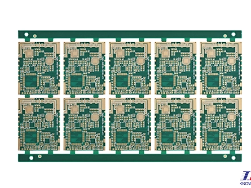
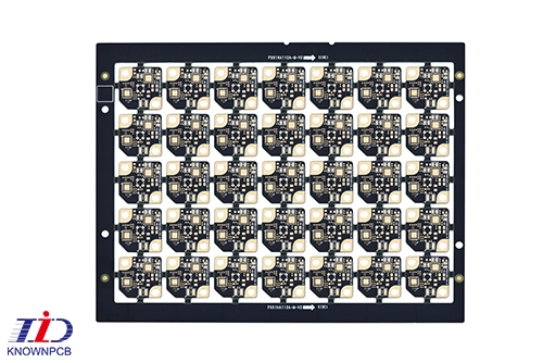
KnownPCB recently delivered a 6-layer high-density PCB panel project with a minimum hole size of 0.15mm. The entire panel is made up by multiple small-sized high-density PCB module units.
In this multilayer high-density board project, we need to precisely control the reliability of extreme micro mechanical via (min. 0.15mm), fine line widths/spacing (min. Track 3/3mil) and hole wall copper (25μm) in a large-area PCB panel structure, as well as ensure the overall board yield and the consistency of mass production for this high precision board. This demands higher requirements on the manufacturing capabilities of PCB manufacturers.
Basics parameters of this 6-layer high-density PCB:
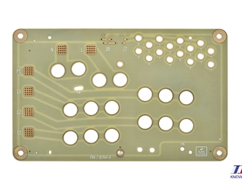
PCB Dimension 164*162mm PCB Thickness 1.6 mm Material Type of PCB FR4 TG150 PCB Surface Finish ENIG 2U PCB Color Black
1. Manufacturing instability of small holes
High-speed drilling of 0.15mm fine via will easily cause drill bit offset and hole misalignment. For multilayer high-density PCB, the drill bit offset will lead to insufficient pad annular ring width or interlayer registration failure. In the meanwhile, the heat that generated in the drilling process may affect the quality of hole wall and reduce electrical conduction reliability.
2. Copper Coverage and Uniformity in Plating
In the electroplating process of this high-density PCB, the exchange capacity of the electroplating solution inside the holes is limited, therefore, the copper in vias may be distributed unevenly, and result in fluctuations in the conduction resistance.
3. Combined Risks of Fine vias and Lines
When 0.15mm small hole coexist with 3/3mil fine line in this high-density board, manufacturing diffciculty increases significantly. On the one hand, interlayer alignment deviations may reduce the spacing between the vias and the circuit lines, on the other hand, the enhanced electroplating process to ensure hole copper quality will also inevitably increase the difficulty of corrosion control for fine circuits.
Additionally, yield risks of fine mechanical vias in a high-density PCB can also exist in via cleaning, high aspect ratio structures and interlayer registration control.
Therefore, to ensure the yield and reliability of this 6-layer high-density PCB panel with 0.15mm small size vias, KnownPCB as a professional PCB manufacturer, have adopted the following manufacturing solutions:
1. First of all, we optimized the drilling process parameters in the pre-production stage, and used high-precision drilling equipment to control the consistency of via position and shape, in order to maintain the the precision of fine via drilling processing.
During the production of this multilayer board, we stabilized the spindle speed and feed rate to reduce via deviation, and ensured the processing stability of the small hole structure from the beginning.
This entire measures provide a reliable premise for the subsequent electroplating process.
2. Secondly, to solve the the insufficient electroplating coverage of fine via, we employed a high-coverage plating process and carried out targeted optimization on the electroplating parameters to enhance the solution exchange inside the holes.
By using this precise process control on this high-density PCB, we have ensured that the copper thickness of the hole walls of this multi-layer high-density panel uniformly all reaches 25μm.
3. We conduct a collaborative optimization from both engineering and manufacturing ends for the coexist of 0.15mm samll size vias and 3/3 mil fine circuits. Through multi-process collaborative control, we prevent the combined effects of hole misalignment, plating variation and etching deviation, guaranteeing stable uniformity and high production yield for this PCB panel with 0.15mm fine vias under extreme manufacturing conditions.
In the result, this high-density PCB panel with 0.15mm mechanical via achieves 25μm hole copper thickness and 3/3 mil fine lines. Meanwhile, this boards maintained outstanding consistency across all panel units, and met the stability demands of batch SMT assembly.
Request for a tech support