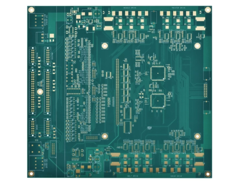
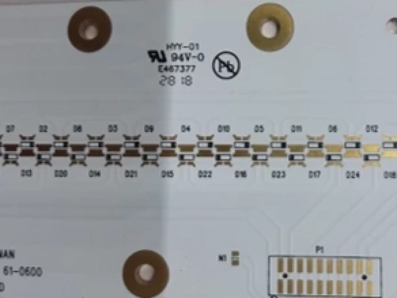
KnownPCB delivered a project of 22-layer heavy copper PCB for high-power DC power supply, which is the ultimate answer to complex thermal challenges. By utilizing massive 4oz inner copper weights, heavy copper layers act as integrated heat sinks to boost power efficiency.
Thanks for our superior lamination reliability.
Core Specs of the heavy copper PCB: 22 Layers | 4oz Inner Copper | 2oz Outer
Precision Engineering: 7.87mil/7.87mil minimum trace/space
| type of PCB | Heavy Copper PCB with 22 layers 2 pressed and buried blind holes |
| PCB Dimension | 36.8mm*58.4mm |
| PCB Surface treatment | ENIG (immersion gold) |
| Thickness of the PCB | 5.2±0.4mm |
| Applications | High-power DC power module |
High current is a big deal.
Without sufficient copper weight, PCB turns into an "electric blanket" in minutes.
How to make a decision on the materials?
Using Taiyao Tu865 plate, the heavy copper foil design can withstand the high voltage and high current loads of high-power DC power supplies, providing a low-resistance current channel, reducing power loss and heat generation, and maintaining good stability and reliability.
Performance Benchmark: At 20A, KnownPCB’s 3oz copper maintains a modest 58°C rise, whereas standard 1oz copper spikes to 105°C, risking component damage. Don't settle for "good enough." Choose the board designed for uninterrupted 24-hour performance.
Request for a tech support
October/13/2025China-based High-current Industrial PCB Manufacturing Project
November/12/2025High-frequency Bare PCB | Industrial PCB Manufacturing

April/14/2026Do you really understand via pads?
March/17/2026What is a metal core pcb in industry?

March/17/2026SMT Reference Board with Specialized PCB Fabrication
