Get A Quote
CN
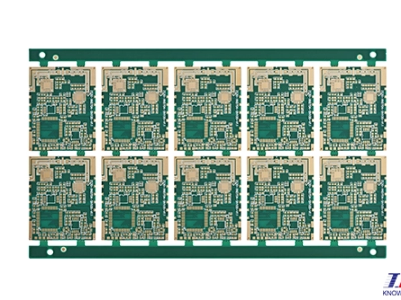
Recently, KnownPCB have completed a project of 6-layer heavy copper PCB with multiple types of plated through-hole structures. The through-hole structure on this multilayer heavy copper board is the key feature of the interlayer connection and high-current conduction.
While ensuring optimal thermal management of this kind of heavy copper board, we using our uniform through-hole plating process to achieve robust through-hole plating quality which complies with IPC Class 3, and further more improve interconnection reliability and mechanical stability of this multilayer heavy copper PCB under high current load conditions.
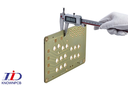
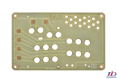
Technical parameters of the heavy copper PCB:
| Type of PCB | 6-Layer Heavy Copper PCB |
| PCB dimension | 260*160mm |
| PCB surface treatment | ENIG |
| Thickness of the PCB | 5.77mm |
| Applications |
High current distribution block |
If the copper thickness of the hole wall is non-uniform, it will easily increase the electrical resistance and local temperature inside the board, and lead to failures such as barrel cracking or corner fractures under thermal cycling conditions, thereby affecting the stability and long-term reliability of high-current transmission.
Since the risks are coming from non-uniform hole wall copper thickness, thus, the critical goal in manufacturing control of multilayer heavy copper PCB is to enhance plating uniformity and coverage.
Therefore, KnownPCB address this heavy copper board manufacturing challenge in through-hole plating:
We used high-coverage electroplating process, and with optimized current distribution and accurate process control to achieve consistent hole-wall copper thickness. This measure ensures the thick copper board can still maintain robust interconnection reliability under high-current loading and repeated thermal cycling.
Since 2008, KnownPCB has focused on multilayer heavy copper PCB fabrication with large-diameter through holes. We have continuously gathered fully experiences in thick heavy copper board production processing, uniform through-hold plating, and thermal management.
Request for a tech support
KnownPCB Production Lines
KnownPCB Industry Solutions
Submit Your Gerber
Request Stackup Review

March/17/2026Heavy Copper PCB with Complex Shape Machining for High-Current Applications
April/29/2026The Pad Consistency for The Fine-Pitch BGA PCB
March/17/2026What is a metal core pcb in industry?
April/22/2026How Do Via Stubs Affect Signal Integrity in High-Speed PCB?
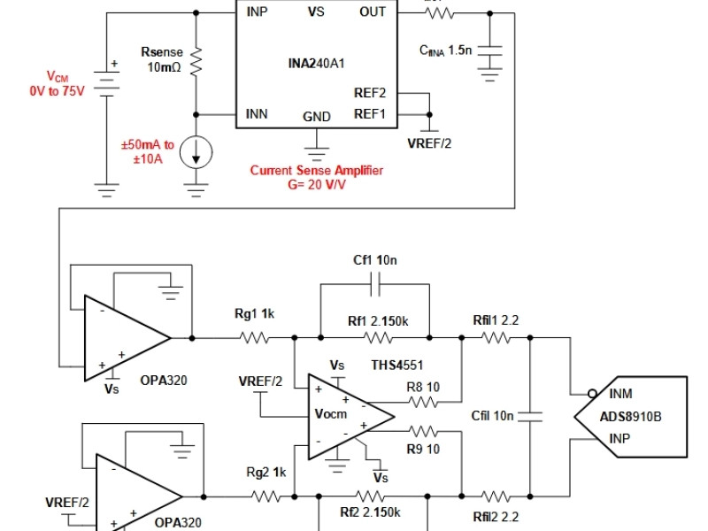
June/09/202610A Battery Current-Sense PCB
