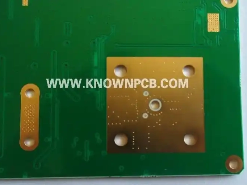
A successfully DFM and process control for the Large-Current Board(high-current PCB).
When engineering an active energy-storage BMS or pack monitoring system, handling a continuous 10A load while maintaining an 18-bit sampling resolution introduces a multidimensional challenge. The layout cannot simply be treated as a standard power plane; it must balance the heavy-copper thermal escalation with a ultra-low-noise micro-volt digitization chain.
The specification, such as current range goes up to 10A, the ADC resolution reaches 18 bits, and the front-end bandwidth covers 0–10kHz, mean that the Large-Current Board already touch PCB manufacturing, assembly, testing, and calibration.
Article SummaryThis blog uses a 10A battery current-sense PCB as a practical case to explain how a complete DFM review for a high-current PCB should be handled before prototype, small-batch production, and mass production.
|
Article Contents |
In battery test equipment, energy-storage BMS, and industrial power systems, current-sense boards requires solving three bottlenecks at the same time: the high-current power path, the precision analog front end, and production consistency in high-current PCB.
When a design demands a 10A current with 18-bit sampling accuracy and 0–10kHz front-end bandwidth, the PCB design constraints of the high-current PCB well into the realms of manufacturing, assembly, testing, and calibration.
10A Current PathPractically, the 10A current path has to keep temperature rise under control during continuous operation. | μV-Level Sensing ChainThe Current Shunt sensing path has to keep errors low while dealing with μV-level signals. | Production ConsistencyFrom small-batch runs to mass production for high-current PCB, solderability, testability, and calibratability remain consistent across all PCB production scales. |
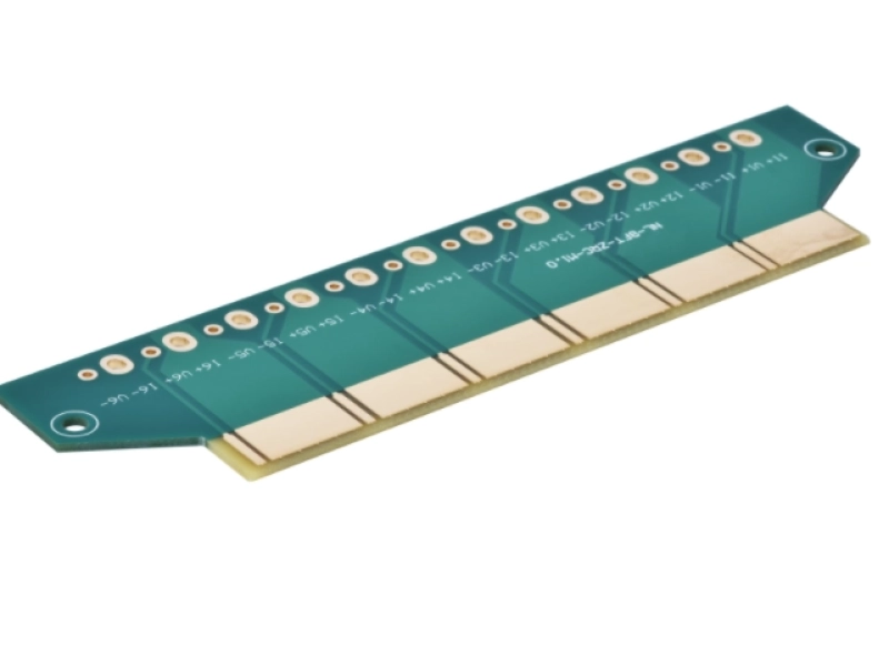
Rsense serves as the primary sensing element of the high-current PCB. When a 10mΩ shunt carries a 10A current, the resistor dissipates about 1W of power, spreading heat across the PCB through the pads and copper areas. HOT SPOTS, THERMAL Gradient, Kelvin SensingThe inadequate copper width leads to local hot spots along the main current path. The thermal gradient will cause drift on account of the non-symmetrical copper on the two sides of Rsense. Furthermore, the Kelvin sensing points must be precisely defined; otherwise, the ADC front end will also pick up parasitic voltage drop on the copper. | 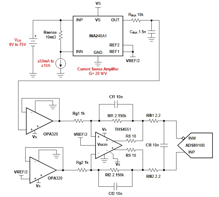 |
KNOWNPCB would cover:
|
These PCB constraints for battery test equipment or energy-storage BMS applications directly affect full-scale accuracy, zero drift, and batch-to-batch consistency.
KNOWNPCB audits the input terminal, section by section: connector, copper area, vias, Rsense, and return path for the 10A main current path. Any neck-down, single via, uneven copper shape, or too-small pad can become the place where temperature rise and voltage drop pile up.
| Item | DFM focus |
| 10A main current path | Whether the trace or copper width meets the temperature-rise requirement, and whether there is any neck-down. |
| Copper thickness | 2 oz outer-layer copper is recommended; temperature-rise estimation should be done at least during the prototype stage. |
| Vias | Use multiple vias in parallel for layer transitions; don’t let one via carry the whole story. |
| Connector pads | Whether pad area, copper connection, and mechanical strength match the 10A input requirement. |
| Copper on both sides of Rsense | Keep the copper areas as symmetrical as possible to reduce thermal gradients. |
| Solder mask opening | For the shunt resistor and high-current copper areas, solder mask openings may be evaluated to improve heat dissipation. |
The copper width of a high-current-sense PCB is not only about current-carrying capacity. It also shapes the temperature distribution around the shunt resistor. When the temperature is uneven, Thermal non-uniformity introduces extra errors across the low-value sense resistor, solder joints, and copper. And yes, those errors finally show up in the ADC readings.
KNOWNPCB elevates the Rsense connection from a “nice-to-have” method to a hard layout constraint. The Kelvin sensing path picks up the real voltage drop across Rsense with a 10A main path. These two paths cannot be mixed.
For any precision 10A battery current-sense PCB, four-terminal Kelvin routing topology is non-negotiable. If the differential feedback traces pick up even a fraction of a millimeter of the high-amp track's parasitic resistance, the resulting I X R voltage drop will obliterate the accuracy of your high-resolution ADC.
| Item | Inspection requirement |
| Kelvin sensing point | Route from the effective sensing terminals of Rsense, or from the inner pads. |
| Sense trace length | Keep it as short as possible and close to the current-sense amplifier. |
| Sense trace geometry | Differential, symmetrical, and tightly coupled. |
| Sense trace environment | Keep away from switching nodes, digital clocks, and high-current return paths. |
| Reference ground | Keep a continuous ground plane under the analog signals. |
| Component placement | Place Rsense, CSA, FDA, and ADC compactly along the signal chain. |
Engineering NoteThe bottom-line: Kelvin sensing is part of the measurement chain, that is a fundamental principle for an 18-bit current-sensing system. Per KnownPCB’s engineering standard, when we run the DFM review, we need to keep out the Layer 2 ground plane directly under the THS4551’s input pins and feedback traces. Reason: A pole is introduced by the parasitic capacitance acting with the 2.15kΩ feedback resistor. In a 10kHz system, especially with high-frequency switching or PWM interference around, this may cause self-oscillation or overshoot. |
While expansive heavy-copper matrices are excellent for mitigating Joule heating, they act as massive thermal sinks during the production reflow phase. An unoptimized PCB fabrication audit (DFM) leads to unbalanced thermal mass on the sampling resistor pads, widening the risk of cold solder joints and component shifting during automated assembly.
Around Rsense, it requires an optimized DFM approach to find the sweet spot between heat dissipation and solderability, here is the checking list:
| Item | DFM focus |
| Rsense pads | Whether they follow the device manufacturer’s recommended footprint. |
| Large copper connection | Whether to use solid connection or thermal relief should be evaluated based on both current carrying and solderability. |
| Copper symmetry | Keep the thermal mass on both sides as close as possible to reduce soldering offset and thermal drift. |
| Solder mask opening | Whether the exposed copper area improves heat dissipation, and whether it affects solder spreading. |
| Stencil aperture | Windowpane apertures may be considered for large pads to reduce voids and solder-volume variation. |
| AOI inspectability | Whether the solder-joint edges can be seen. |
| Rework clearance | Whether enough working space is reserved around the shunt resistor and connectors. |
During the high-current PCB prototype stage, hand soldering can bail engineers out of some layout flaws. But once the high-current PCB project transit to small-batch production, pad thermal balancing, stencil apertures, and the reflow profiles become the ultimate drivers for process consistency.
During the high-current PCB prototype, KNOWNPCB gives priority to checking:
| For high-current PCB small-batch and mass-production stages, more items need to be added:
|
As the high-current PCB project moves from prototype validation to volume production, it becomes “can this high-current PCB be replicated reliably at scale?”. When it comes to high-current precision sensing PCBs, getting this step right is what saves PCB project owners from high test costs and endless reworks down the road.
Given the combination of a 10A current path, 18-bit sampling accuracy, and 0–75V input environment, KNOWNPCB recommends reviewing this type of high-current PCB according to the following process requirements:
| Item | Recommendation |
| PCB type | High-current precision analog current-sense board. |
| Layer count | 4 layers. |
| Material | FR-4, high-Tg preferred. |
| Board thickness | 1.6 mm. |
| Outer-layer copper thickness | 2 oz recommended. |
| Inner-layer copper thickness | 1 oz. |
| Surface finish | ENIG preferred. |
| Minimum trace width/spacing | 4/4 mil or 5/5 mil. |
| Impedance control | Usually not mandatory. |
| HDI / blind and buried vias | Usually not required. |
| High-current area | Wide copper, multiple vias, and solder mask openings where necessary. |
| Rsense area | Kelvin sensing, symmetrical copper, and heat-spreading copper. |
| Analog front end | Short routing path, continuous ground, and separation from digital noise. |
| Test points | Support ICT/FCT, calibration, and debugging. |
ConclusionWhen reviewing a high-current PCBs, we look at the whole picture: start from the current path, then move into thermal distribution, sensing error, soldering stability, and production testing. For the 10A battery current-sense case, trace width and copper thickness are baseline qualifiers. Rsense Kelvin sensing, copper symmetry, pad thermal balance, ADC front-end layout, test points, and calibration procedure are the things that decide whether a high-current PCB prototype can move smoothly into mass production. The earlier the engineering team bakes high-current PCB DFM rules into the PCB constraints and production process documents, the lower the risk of late-stage debugging, rework, and batch-to-batch variations. |
KnownPCB’s engineering philosophy drives us to view DFM not a binary check of “Can this high-current PCB be made?” for precision high-current boards, it must transcend basic fabricability- soldered consistently, tested consistently, calibrated consistently, and produced consistently at scale. To mitigate risks effectively on 10A battery sensing PCB boards, KNOWNPCB recommends early engagement with the PCB factory to review the current loops, Kelvin sensing, copper thermal balance, test points, and production process requirements. That way, high-current PCB manufacturing risks can be caught earlier, cutting down on prototype re-spins, pilot-run troubleshooting, and volume yield instability. |  |
Need DFM Support for a High-Current Sensing PCB?Send your Gerber files, stack-up, BOM, current path requirement, test requirement, and calibration notes. KnownPCB can help review the manufacturability and production process risks for your high-current PCB project.
|