Designing and Manufacturing a High-Speed Data Acquisition 4-Layer PCB: A Deep-Dive DFM & DFA Review
By the Engineering Team at KnwonPCB
high-speed data acquisition 4-layer PCB design and manufacturing review
Article Navigation
1. Project Breakdown & Design Insights
2. Factory DFM Check: Design & Process Compatibility
3. Power Delivery & Ground Systems
4. Assembly & Testability (DFA Review)
5. Production Feasibility & Risk Mitigation Matrix
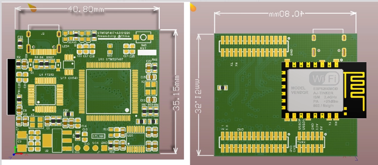
Let’s look at what we’re dealing with here: This 4-layer PCB project is ahigh-performance embedded development and data acquisition (DAQ) PCB designedspecifically for small-to-medium production runs. As a typical early-stage PCBprototype engineered to validate R&D concepts before full-scalemanufacturing, this design serves as an excellent case study for advanced DFM(Design for Manufacturability) and DFA (Design for Assembly) reviews.
But don’t let the size fool you. Designing this thing comes with some real engineering challenges. You’re trying to pack a 4-layer PCB stackup, a high-speed mixed-signal layout, tight-pitch connectors, and controlled impedance all into one small, restricted footprint.
Here is a quick breakdown of the core design features for the high-Speed Data Acquisition PCB:
4-layer PCB stackup with high-speed digital and analog signal routing
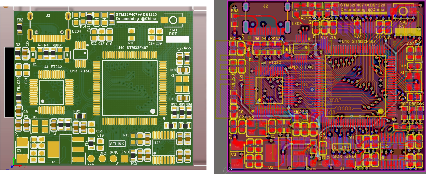
Based on this High-Speed Data Acquisition PCB layout features, here is what our team focuses on when evaluating whether 4-layer PCB is actually ready for the factory floor.
What we found in the 4-layer PCB design:
PCB Factory DFM Technical Feedback from KnownPCB:
Stackup Optimization for High-speed Data Acquisition 4-layer PCB
We will take your 50Ω single-ended and 100Ω differential impedance targets and run them through our system. We'll map them against our standard stock material—like Shengyi S1000-2 (High-TG FR4)—and adjust the core and prepreg thicknesses to make sure the board can be built reliably within our standard factory process window.
Also, since the design mentions a 0.4 mm (around 16mil pitch near the inner layer dense areas, we need to make sure things aren't too tight, which could risk crosstalk or etching yield issues.
The documentation points to a conventional process limit of 4mil for trace width and spacing. We'll need to scan the entire Gerber package to make sure no high-speed lines drop down to something like 3mil without warning. The breakout areas right near those high-density connectors are the most vulnerable spots where spacing rules usually get violated, so we’ll be watching those closely.
We need to check the finished hole size (FHS) against the pad size for all vias and through-holes. To prevent the drill from wandering and causing an annular ring breakout, we need to ensure the solder ring has enough copper on one side (usually ≥ 0.1 mm). This is especially critical if the STM32F4 comes in a BGA package where via-in-pad might be required.
The schematic shows the analog power connecting to the 3.3V rail via a ferrite bead (R12), which is a classic, solid way to isolate analog and digital domains.
On the physical layout, we need to check that the split between the analog power/ground planes and digital power/ground planes is clear. The isolation bridges need to be placed sensibly. If you end up with an accidental "dumbbell" shape split plane, return paths will get cut off, forcing signals to loop all the way around the board, which completely ruins signal integrity. We will specifically double-check the copper area right under the ADS1220 chip to make sure it hasn't been sliced up by an incorrect dividing line.
Capacitors work best when they are physically close to where the action is. We will check the layout to make sure there are enough decoupling caps placed right next to the power pins of the STM32F4, FT232H, and ADS1220. Vias should be punched directly near the capacitor pads to form the smallest possible return loop; long traces between the cap and the pin defeat the purpose.
We will audit the component footprints, especially the fine-pitch QFN/LQFP packages for the STM32F4 and FT232H. If pads are too large, parts will float around during reflow and cause shorts; if they are too small, you get weak joints or "tombstoning" (where a component stands up on one end).
A Quick SMT Compliment: > Using an asymmetric pin header design to prevent users from plugging things in backward is an excellent DFA practice. We love to see this, and we’ll make sure our assembly line sets it up flawlessly.
We will make sure all designators, polarity marks, and port labels (like USB, TX/RX) are crisp and clear. Most importantly, we’ll ensure no silkscreen overlaps with the exposed copper pads, as printing ink onto a pad will ruin the solder joint.
For a development PCB, debug access is everything. Are there test points for the main power networks (5V, 3.3V, 1.2V) Are the serial debugging pins easy to reach? Our factory flying probe testing—and your own desktop debugging—will depend heavily on these.
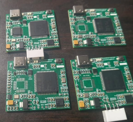
PCB assembly
Overall, this High-Speed Data Acquisition PCB looks very buildable, but a few manufacturing specs need to be locked in before we spin the wheels.
| Project Item | Our Factory Perspective & Action Plan |
|---|---|
| Surface Finish | We strongly recommend ENIG (Electroless Nickel Immersion Gold) for this development PCB prototyping. It provides a perfectly flat surface, which is crucial for soldering the fine-pitch USB bridge and pin headers. Plus, it handles repeated manual soldering, insertions, and probing much better than standard Lead-Free HASL. |
| PCB Materials | We will use high-quality High-TG FR4 (TG150 or TG180) from trusted brands like Shengyi. This stops the 4-layer PCB from warping during lead-free reflow cycles. Copper thickness will be standard 1oz 35µm) for both inner and outer layers, and everything will be built to meet IPC-A-600 Class 2 standards. |
| Stencil & Reflow | We will laser-cut stencils customized to this specific PCB file. For the precise analog section around the ADS1220, we’ll use fine-grain SAC305 lead-free solder paste and fine-tune our reflow oven curve to match the component specifications perfectly. |
| Analog Precision Clean | To keep the ADS1220’s analog front end (AFE) free from electrical leakage, the High-Speed Data Acquisition PCB will go through a thorough washing cycle post-SMT to eliminate flux residues and contamination. |
To save time and avoid extensive rework later, keep these four factory tips from KnownPCB in mind:
At the end of the day, the overall quality of this design project is great. This isn't amateur work; it’s clear the designer thought through basic SI and DFM rules, which sets a rock-solid foundation for a clean production run.
The next step is simple: let's connect, lock down the exact impedance calculation numbers based on our S1000-2 material stackup, and do a quick pre-production review. Once that's cleared, we're ready to hit the factory floor and build a fantastic multilayer PCB.
March/18/2026Via-in-Pad Resin Plugging in High-Voltage PCB
October/27/2025Custom Thermally Stable PCB | Industrial PCB Manufacturing
April/21/20268-Layer BGA PCB with VIPPO technology
April/20/20268-layer HDI PCB with Edge Connector
March/17/2026High-Frequency PCB with FR4 & Rogers Hybrid Lamination
