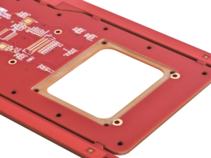
This Project is about a 4-layer high-voltage PCB with via-in pad structure for industrial control applications which recently delivered by KnownPCB. In this multilayer high-voltage board, the via-in-pad construction is applied in the pad areas of key components and we used resin plugging process to ensure superior pad flatness and long-term structural stability.
For such high-voltage circuit board design, via manufacturing technology affects both soldering quality and the long-term reliability of the entire board in high-voltage operating environments.
The parameters for this custom high-voltage PCB:
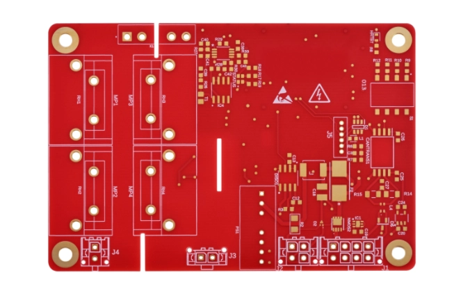 | Base Material | S1600 |
| Layers | 4 | |
| Dimensions | 90*65 | |
| PCB Thickness | 1.6 mm | |
| Board Solder Mask Color | Red | |
| Silkscreen | White | |
| Surface Finish | ENIG 2U'' |
View more Product Line | View more Project Solution
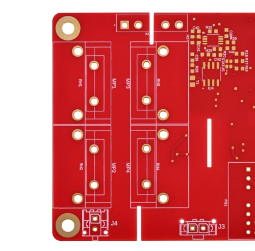
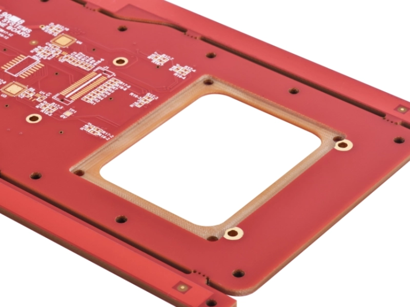
For via-in-pad structure, vias are placed in the center of pads. Therefore, if there is any improper via processing during this high-voltage board manufacturing, when the circuit board is soldering through reflow process, molth solder will easily flow into the via holes, which can leads to typical assembly failures such as solder voids, dry joints and pad collapse.
For this multilayer high-voltage PCB, the density and structural stability of internal via filling also influence the long-term reliability
2. Pad flatness risks: Pad depression or uneven surface, which affects mounting stability of SMT placement.
3. Filling defects: insufficient filling, shrinkage, or internal void risk
Since the main challenge of this 4-layer high-voltage PCB is from the soldering and structural risks which caused by improper via treatment, thus, the key point for the solution of manufacturing is:
Improve the compactness of via filling and the surface flatness of pads, in the meanwhile ensure structural thermal stability.
To solve this challenge, KnownPCB adopted the via-in-pad resin plugging process with stable manufacturing quality through the control of key process parameters:
1.We achieve a filling rate of nearly 100% to ensure the internal structure of vias is dense and does not have obvious voids.
2. By controlling the surface flatness of the pad area within ≤20μm, we guarantee the SMT stability for this high-voltage board.
3. we optimized the resin curing process, and reduce the risk of pad depression caused by material shrinkage.
Request for a tech support
October/27/2025Industrial 2-Layer FR4 PCB Manufacturing| Red Solder mask | Hard Gold Finish
April/22/2026How Do Via Stubs Affect Signal Integrity in High-Speed PCB?
March/25/2026Industrial Control PCB with Hard Gold 15U
June/09/202610A Battery Current-Sense PCB
April/21/2026Uniform plating in Heavy Copper PCB
