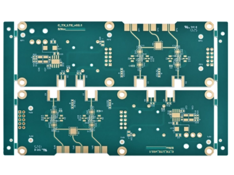
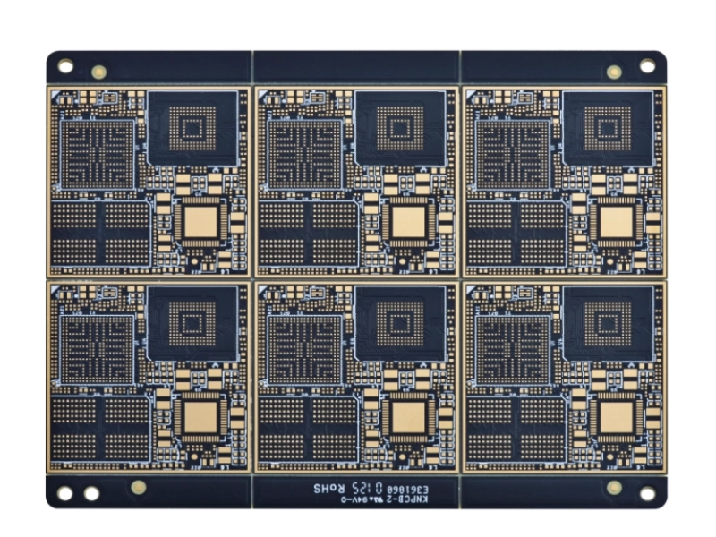
This 6-layer high-speed PCB with back-drilling structure was custom-made for our client previously before.
During the manufacturing of this multilayer high-speed board, the biggest challenge was the precise back-drilling depth control to eliminate via stubs, and maintain excellent high-speed signal integrity across the entire high frequency circuit board.
The required process parameters for this 6-layer high-speed PCB with back drill are as follow:
| PCB color | Green |
| PCB surface treatment | ENIG |
| Thickness of the PCB | 1.2 mm |
| PCB material Type | Rogers RO4003C |
A via stub is the excess conductive segment in a via that does not participate in signal connection. In high-frequency and high-speed PCB designs, via stub will cause signal reflection and impedance discontinuity, consequently have negative impact on signal integrity of high-speed board.
Back drilling is the best and cost-efficient way to remove via stubs by secondary drilling from the reverse side of the high-speed board, Nevertheless, just using back drilling might not ensure better signal quality, it will also rise risks of manufacturing at the high-speed PCB.
In conclusion, the key determination is the precise control of back drilling depth during high-speed and high-frequency PCB manufacturing.
As a experienced and reliable manufacturer of high-speed and high-frequency PCBs, how do KnownPCB accurately control the depth of back-drilling and via stub length to achieve a stable and consistent high-speed signal path structure?
Solution: During the DFM reviewing of this 6-layer high frequency PCB, we have confirmed with our client about the target back-drilling layers, depth, and tolerances. For high-speed and high-frequency boards, the deviation of back-drilling depth should be strictly controlled within ±0.025 mm.
After the production of this multilayer high-frequency board, we verified the via stub length is ≤ 0.05 mm through the cross-sectioning. This shows excellent back-drilling performance and successfully reduces the risks of high-speed signal reflection and transmission loss.
Solution: Similarly, we have comfirmed the interlayer safety clearance with our client in pre-production DFM review and conduct multi-point thickness measurements before the fabrication of this 6-layer high frequency PCB. By considering the fluctuation of PCB thickness may be ±0.05 mm within the same batch, we have adjusted the back-drilling depth based on actual board thickness, bit calibration, and wear compensation. This measures ensured a minimum safety margin of 0.03 mm between the back-drilled base and the target internal layer.
Solution: In order to reduce the risk of back-drilling offset in this multilayer board, we use high-precision drilling mashine which is equipped with CCD optical alignment and closed-loop depth control to compensate for substrate dimensional variation and realize precise location.
This high-precision drilling machine achieves Z-axis positioning precision of ≤±0.01 mm and will automatically shut down with an alert if depth error exceeds ±0.03 mm.
With precise control for back-drilling depth and via stub length in high-frequency board, KnownPCB delivers outstanding high-speed signal integrity while maintaining signal path structural reliability. We provide stable and reliable manufacturing solutions for high-frequency and high-speed PCB applications.
Request for a tech support