Serving US and North American OEMs under NDA-backed intellectual property protection.

WE BUILDHigh-density interconnect boards for
| WE OFFER
With IPC-compliant, RoHS/REACH-ready materials. All projects are supported by our English-speaking engineers. |
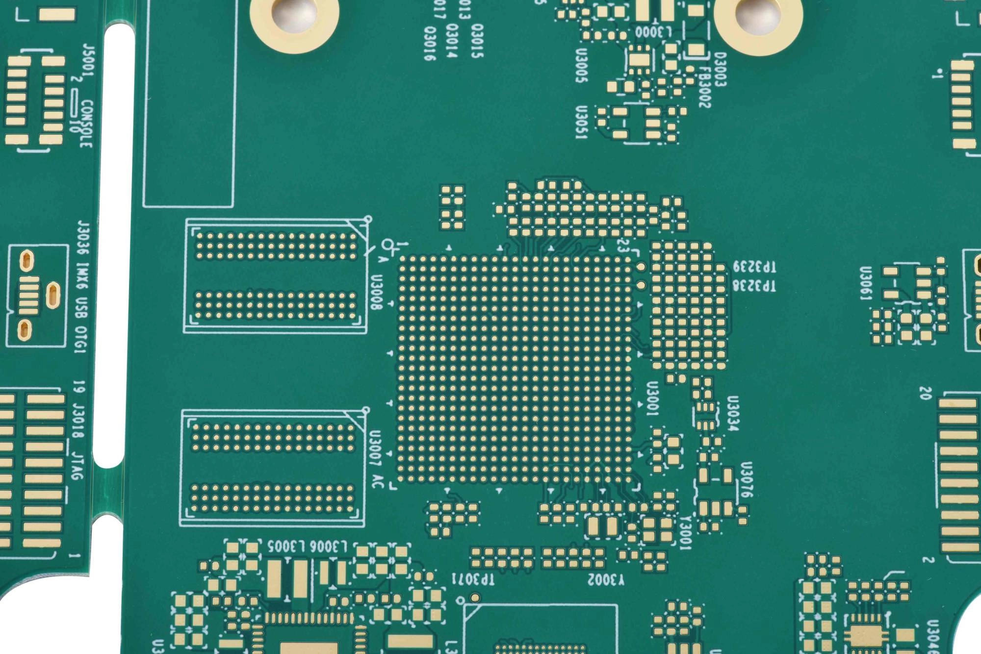
High-density interconnect board (or multilayer HDI PCBs) with fine line/space, microvias, and via-in-pad for fine-pitch BGAs.
Qualification Materials & Compliance OverviewAcceptance StandardsThese materials were tested according to IPC-6012 criteria as well as internal HDI criteria such as microvia reliability testing, thermal cycling tests and IIR thermal cycling simulation. Material StandardsHDI-capable FR-4 or low-loss materials with controlled CTE; laser-drillable, via-fill compatible dielectrics. Structure OverviewSequential build-up layers with stacked or staggered microvias, blind/buried vias and via-in-pad connections. ComplianceDesigned to meet RoHS / REACH, UL recognition, and OEM-specific HDI design rules for long-term reliability. |
KnownPCB Prototyping & Mass Production Service Ask for DFM Guideline
Higher bare-board price, optimized for dense layouts and small form factors.
|  |
| Strong interconnect quality for high-speed and high-pin-count devices.
|
KnownPCB Prototyping & Mass Production Service Ask for DFM Guideline
HDI fabrication demands sub-mil micron precision for interconnects. We achieve this using LDl lmaging for fine-line circuitry and Laser Drilling for microvias. Critical tolayer stacking is the X-Ray Alignment System, ensuring precise registration before Sequential Lamination. Every layer is confirmed via AOI Inspection to guarantee reliability and density. KnownPCB Profile Ask for Key Design Consideration Guideline | 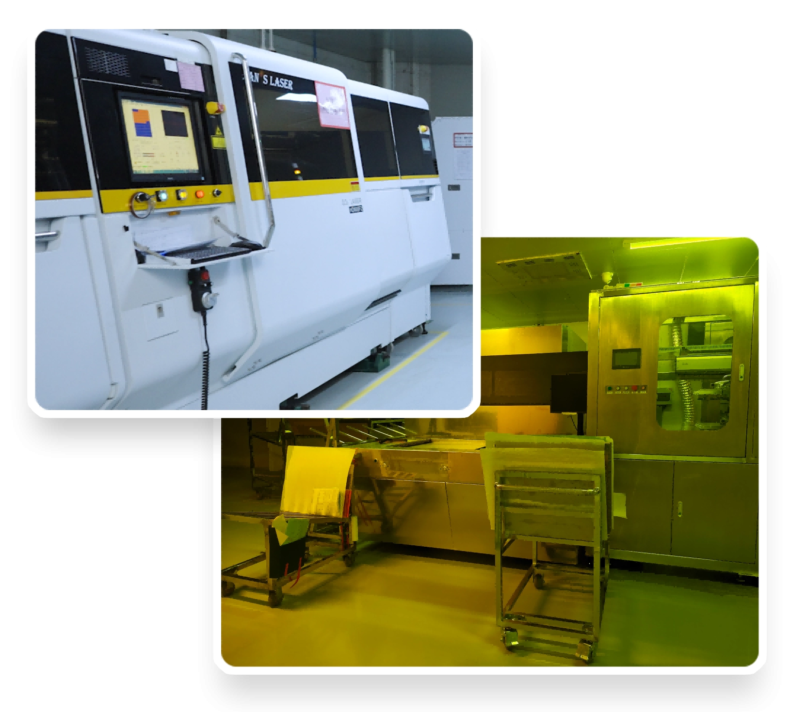 |
| Parameter | 1-step HDI | 2-step HDI | 3-step HDI | Any-layer / ELIC | Engineering Reference |
| HDI Build-up Structure | 1+N+1 | 2+N+2 | 3+N+3 | Full any-layer interconnect (ELIC) | Stack-up definition / design basis |
| Typical Blind-via Pairs | L1–L2 | L1–L3 / L(n)–L(n–2) | Multi-stage stacked microvias | Any-layer interconnect | Process selection |
| Microvia Type | Staggered (recommended) | Staggered + partial stacked | Fully stacked (multi-level) | All-stacked / any-layer | Reliability / solder quality |
| Via-in-Pad (VIPPO) | Optional | Common for BGAs | Mandatory for high-density BGAs | Mandatory for RF/high-speed | Packaging / BGA breakout |
| Skip Via (Learn about Via Protection Types) | Not recommended | Optional | Common | Fully supported | Shrinks routing channel / saves space |
| Build-up Material System | RCC (thin dielectric) | RCC + PP hybrid | Multi-layer RCC + high-Tg PP | Premium RCC / mSAP | Hole quality / dielectric matching |
| Dielectric Thickness for Build-up | 75–100 μm | 50–75 μm | 50 μm | 25–50 μm | Laser via formation / impedance |
| HDI DFM Rules | Basic routing rules | BGA fan-out required | High-speed / RF DFM constraints | Mandatory high-speed DFM | Manufacturability / reliability |
| Category | Parameter | 1-step HDI | 2-step HDI | 3-step HDI | Any-layer / ELIC | Engineering Reference |
| Layer Count | Total Layer Count | 4–8 layers | 6–12 layers (typ. 8L) | 8–14 layers (typ. 10L) | 12–30+ layers | Stack-up / structure |
| Board Thickness | Min Thickness | 0.012" (0.3mm) | 0.016" (0.4mm) | 0.016" (0.4mm) | Per design | Stack-up / reliability |
| Max Thickness | 0.200" (5.0 mm) | 0.250" (6.35 mm) | 0.300" (7.6 mm) | Per design | Structural limits | |
| Laser Via | Min Diameter | 0.003" (0.076mm) | 0.003" (0.076 mm) | 0.003" (0.076 mm) | 0.05–0.15 mm | HDI drilling |
| Max Diameter | 0.008" | 0.008" | 0.010" | Per design | Stack-up | |
| Aspect Ratio | ≤0.6:1 | ≤0.8:1 | >0.8:1 | Formula: 1 : (0.5 + 0.1×HDI stage) | Via quality / reliability | |
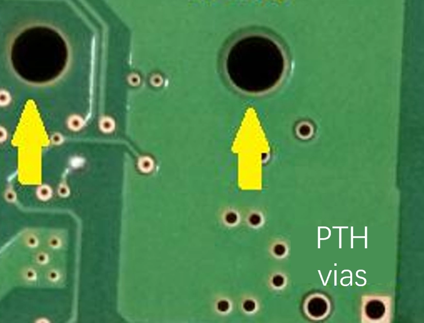
| Mechanical Drill | Min PTH Diameter | 0.006" (0.150mm) | 0.006" (0.150mm) | 0.005" (0.127 mm) | Per design | Drill capability |
| Max Aspect Ratio (Through-hole) | 10:01 | 12:01 | >20:1 | Per design | Plating quality | |
| Trace / Space | Min L/S | 0.004" (0.10 mm) | 0.003" (0.075 mm) | 0.002" (0.051 mm) | Base – (5 μm × HDI stage) | Material / process |
| Copper Thickness | Inner Layers | 0.5–2 oz | 0.5–3 oz | 0.5–4 oz | ↑ Plating with HDI stage | Material / process |
| Outer Layers | 0.5–2 oz | 0.5–2 oz | 0.5–2 oz | Per design | Surface routing |
| Category | Parameter | 1-step HDI | 2-step HDI | 3-step HDI | Any-layer / ELIC | Reference |
| Material Options | Base Materials | FR-4 /SY S1000-2/Rogers/Megtron6 / PI | FR-4 /SY S1000-2/Rogers/Megtron6 / PI | FR-4 /SY S1000-2/Rogers/Megtron6 / PI | High-end FR-4 / Rogers / Polyimide | Material |
| Surface Finish | — | ENIG / OSP / HASL | ENIG / OSP / HASL / Selective Gold | ENIG / OSP / ENEPIG / Soft/Hard Gold | Per design | Material / connector pads |
| Impedance Control | Tolerance | ±10% | ±10% | ±5% | ±5% (mSAP capable) | SI / RF |
| Hole Plating | Blind/ Buried Via Copper | ≥15 μm | ≥15 μm | ≥18 μm | ↑ With HDI stage | Reliability |
| PTH Copper Thickness | ≥20 μm | ≥20 μm | ≥20 μm | ↑ With HDI stage | Reliability | |
| Registration | Layer-to-layer Registration | ±0.003" (0.076mm) | ±0.003" (0.076mm) | ±0.002" (0.051mm) | ±(25 + 5×HDI stage) μm | Stack-up / alignment |
| Warpage | — | ≤0.75% | ≤0.75% | ≤0.7% | ≤0.5–0.7% | Reliability |
| Solder Mask | Min Solder Mask Bridge | ≥0.003" (0.075mm) | ≥0.003" (0.075mm) | ≥0.003" (0.075mm) | ↓ with HDI stage | SMT pad design |
| Min Solder Mask Opening | ≥0.003" (0.076mm) | ≥0.003" (0.076mm) | ≥0.003" (0.076mm) | Per design | SMT pad design | |
| Special Processes | — | Plated via filling, resin plugging | Via fill + resin plugging + LDI | Via fill + resin plug + LDI + embedded copper coins | ELIC, mSAP, all-layer microvia | Material / process |
| Electrical Testing | — | 100% Flying-probe | 100% Flying-probe | Flying-probe + Fixture test | Flying-probe / Fixture + Hi-pot | SI / reliability |
| Lead Time | Standard Cycle | 7–10 days | 8–15 days | 12–18 days | Extended based on HDI stage + layer count | Production planning |
| Reliability Standard | — | IPC-6012 Class 2 | IPC-6012 Class 2/3 | IPC-6012 Class 3 / AEC-Q100 | High-tier optional | High-reliability products |
Industry-specificPCB SolutionsLearn about KnownPCB & Production equipments |
These FAQs are designed to support PCB layout and hardware engineers throughout the entire project lifecycle—from early-stage design clarification and manufacturability questions to production delivery, inspection standards, and storage conditions. KnownPCB acts as a factory consultant, helping you balance cost, lead time, and quality consistency at every stage.
For deeper technical discussions, feel free to reach out to KnownPCB.
Proven by 7 industries, 4000+ customer projects
Please contact us at sales@knownpcb.com, ask for engineering support here or use the form below to reach out to KnownPCB | Get In Touch Today |