A PCB is made up of a core substrate and prepreg (PP) layers laminated together.
The signals and power lines in PCBs often need to move from one layer to another. How is managed the function? Through vias--A via is like a small passage that connects different layers electrically.
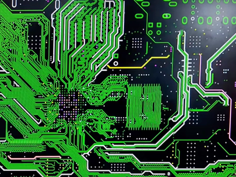
As shown in the figure below, the 6-layer PCB board is designed with the 6L Tier-2 HDI with staggered structure. 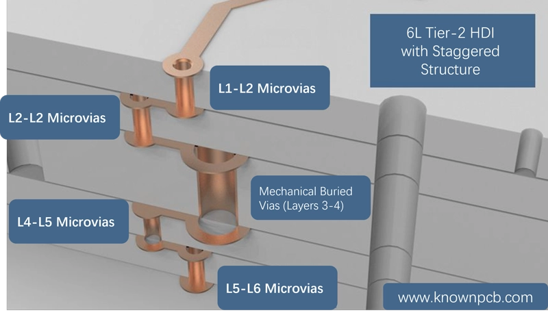 Think of a via in PCB as a channel for signals to move from one layer to another. The function of a via is to provide electrical connection between different layers.
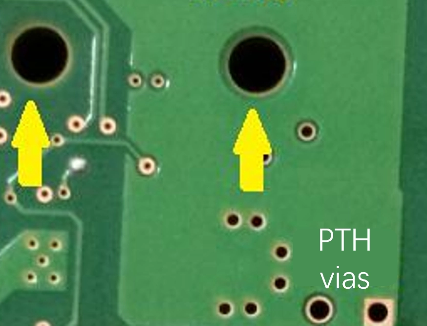
Unlike plated vias, NPTHs in PCBs are used mainly for mechanical purposes, but not provide electrical connection.
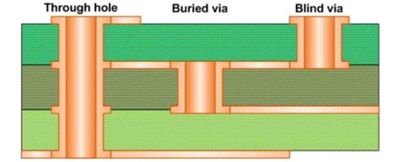
Through holes in Printed circuit boards are the most common type with simple structure and easy processing that leads a high performance in cost.
While through holes in multilayer HDI PCB board is cost-effective and simple processing, it will stop the BGA traces from fanning out properly and space-saving if the PCB layout was designed with lots of BGAs in a dense layouts.
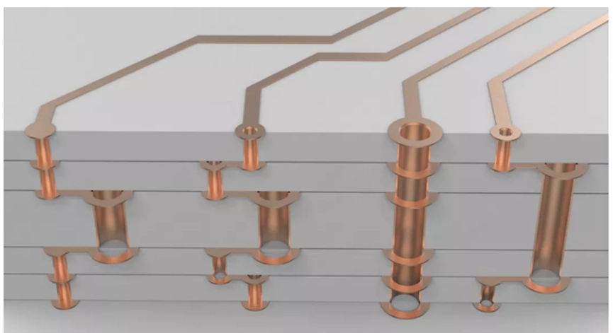
Think of it this way: if the goal is to connect only the fifth and sixth floors of an eight-story building, it makes sense to build a staircase between the two floors, rather than all the way down to the first floor.
Whether it's a simple 2-layer PCB or a complex 20-layer multilayer pcb board, through-holes remain a standard. However, precision comes at a cost: a 0.2mm via is significantly pricier than a 0.3mm one. As the higher cost of labor and tooling are directly involved into the PCB price.
A blind via connects the outer layer of a PCB, either the top or bottom layer, to the nearest inner layer through a plated hole. Since the hole does not be drilled through the entire board, it is called a blind via. In simple terms, you can see the hole from one side of the PCB, but there is no matching hole at the same position on the other side.
A buried via is hidden inside the PCB. The type of via is an internal plated hole that connects only the inner layers of a PCB, but cannot be seen from the outer surfaces. It is a processing of drilled and plated as a premise, then the layers of PCB are laminated together. Buried vias are used for signal interconnection between inner layers and are ideal solution for high-density and high-speed PCB board.
Lasers effectively pierce through fiberglass (FR4 material) resin but stop by copper, ensuring the integrity of internal layers during the drilling process. After the holes are laser-cut and plated, they form laser vias—the backbone of High-Density Interconnect (HDI) technology.
In short, PCB vias are essential for electrical interconnection as channels between different PCB layers.
Among conductive vias, the three main types are through holes, blind vias, and buried vias.
Request for a tech support
 | Download our design guidesfor better PCB designing and manufacturing These are some of the design guides designers and engineersdownload the most:
|
Proven by 7 industries, 4000+ customer projects
Please contact us at sales@knownpcb.com, ask for engineering support here or use the form below to reach out to KnownPCB | Get In Touch Today |